2017.06.23
Graphene, which was discovered in 2005 and awarded the Nobel Prize in 2010, has been so intensely studied due to its high charge carrier mobility, high electric conductivity, superior mechanical strength, excellent chemical stability, and high optical property, and its commercialization has been attempted in various ways and areas. However, despite those strengths, it has been considered hard to be utilized as an electronic material due to the zero bandgap.
Overcoming the weakness of graphene, 2-dimensional (2D) semiconductors, such as molybdenum disulfide (MoS2), began to be investigated and are gaining attention and interest among scientists and engineers.
Unlike graphene, 2D semiconductors have some bandgaps similar to that of silicon and exhibit reasonable charge carrier mobilities. Hence they are expected to become one of the main semiconducting materials for the next-generation electronics. In addition, it is highly probable that they will become an important material for flexible electronics due to the atomic-level thickness.
However, still large-area synthesis or transfer techniques for commercialization of 2D semiconductors are being developed at too slow pace and are at immature stage. Out research team have been developing techniques to grow 2D semiconductors at wafer-scale and to transfer unto flexible substrates and have fabricated high-performance electronic device arrays.
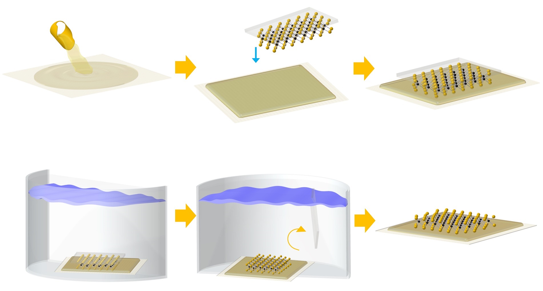
At first, a 2D semiconductor is synthesized at 600 degrees on a silicon substrate and the synthesized film is transferred onto a plastic substrate using epoxy glue. (Refer to figure 1) In this process, the liquid-phase glue is poured onto the plastic substrate and the 2D semiconductor film is glued and cured. Then, the glued 2D material film is separated from the silicon substrate in water. The film is easily separated because of its hydrophobicity. Conventionally, when 2D materials are transferred, the substrate had to be etched or they had to be transferred twice to the final target substrate.
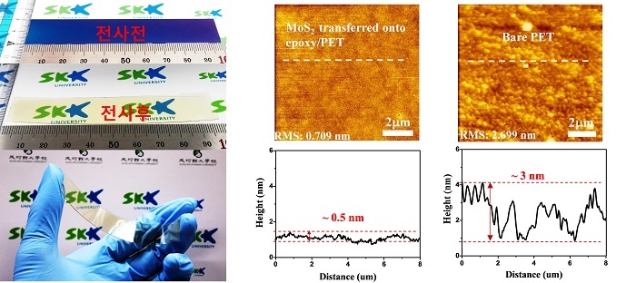
Figure 2. 2D semiconductor before and after transfer. The atomic-level flatness of the transferred film.
During the transfer, the film was damaged due to the chemical corrosion or mechanical stress and the quality was degraded. However, the transferred film of ours did not have any sign of damage, and the quality before and after the transfer was almost identical. This is because the atomic-level flatness is maintained and no residues remain even after the transfer.
This transfer technique can be applied to various 2D semiconductors at large size, used to the fabrication of flexible displays, sensors, and logic devices, and adopted to the commercial mass-production processes.