1 June 2015
Ultrathin ceramic 2D materials can exhibit all kinds of interesting properties, such as superconductivity and magnetism. However, they are not very suitable yet for use in electronics, because of their often limited electrical conductivity. A research consortium, including researchers from UT research institute MESA+, have now found a way to improve the electrical conductivity of these 2D materials by 100 times. Their research has been published in the leading scientific magazine Nature Materials.
At this moment, silicon is the material to be used in semiconductors. Ceramic materials could be an interesting new addition to the semiconductor industry, because they can - by smart constructions - exhibit all kinds of interesting physical properties. For instance, they can be equipped with (combinations of) magnetic, superconductive or, even, insulation properties. Up until now, a limiting factor for the application of ceramic 2D materials in semiconductors is the fact that their electrical conductivity is very limited. Scientists all over the world have been trying to find ways to improve this conductivity for years.
EXTRA LAYER
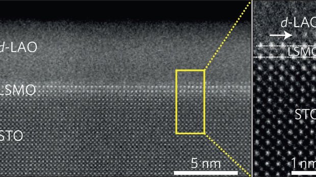
Ceramic 2D materials are made up of several layers. Scientists of an international research consortium have now found a way to improve the conductivity. They did this by separating the layers by an extra layer (composed of lanthanum, strontium and manganese oxide) of just one atom thick. This extra layer ensures that the electrons are separated from defects and therefore can flow through the other lays more easily. This improves the electrical conductivity by 100 times. According to dr. Mark Huijben, who was one of the involved researchers on behalf of the University of Twente, the application of ceramic 2D materials in the semiconductor industry has now moved one step closer. Huijben also is convinced that the improvement of electrical conductivity is an important step for fundamental research, since improved conductivity makes it easier to study physical properties, such as quantum phenomena.
RESEARCH
The research has been conducted by scientists from the Technical University of Denmark, UT research institute MESA+, the University of British Columbia and Canadian Light Source (Canada), the Max Planck Institute for Chemical Physics of Solids (Germany), the University of Antwerp (Belgium), the University of Copenhagen (Denmark), the Max Planck Institute for Solid State Research (Germany) and the Weizmann Institute of Science (Israel). Within the research project, researchers from the University of Twente have focused on measuring the electronic state during the various phases of the fabrication process of the 2D materials in an extremely clean, vacuum environment.
The article entitled “Extreme mobility enhancement of two-dimensional electron gases at oxide interfaces by charge-transfer-induced modulation doping” by Y. Z. Chen, F. Trier, T.Wijnands, R. J. Green, N. Gauquelin, R. Egoavil, D. V. Christensen, G. Koster, M. Huijben, N. Bovet, S. Macke, F. He, R. Sutarto, N. H. Andersen, J. A. Sulpizio, M. Honig, G. E. D. K. Prawiroatmodjo, T. S. Jespersen, S. Linderoth, S. Ilani, J. Verbeeck, G. Van Tendeloo, G. Rijnders, G. A. Sawatzky and N. Pryds, has been published in Nature Materials [DOI: 10.1038/nmat4303].

