August 11, 2013
Researchers at the Georgia Institute of Technology want to put your signature up in lights – tiny lights, that is. Using thousands of nanometer-scale wires, the researchers have developed a sensor device that converts mechanical pressure – from a signature or a fingerprint – directly into light signals that can be captured and processed optically.
The sensor device could provide an artificial sense of touch, offering sensitivity comparable to that of the human skin. Beyond collecting signatures and fingerprints, the technique could also be used in biological imaging and micro-electromechanical (MEMS) systems. Ultimately, it could provide a new approach for human-machine interfaces.
“You can write with your pen and the sensor will optically detect what you write at high resolution and with a very fast response rate,” said Zhong Lin Wang, Regents’ professor and Hightower Chair in the School of Materials Science and Engineering at Georgia Tech. “This is a new principle for imaging force that uses parallel detection and avoids many of the complications of existing pressure sensors.”
Individual zinc oxide (ZnO) nanowires that are part of the device operate as tiny light emitting diodes (LEDs) when placed under strain from the mechanical pressure, allowing the device to provide detailed information about the amount of pressure being applied. Known as piezo-phototronics, the technology – first described by Wang in 2009 – provides a new way to capture information about pressure applied at very high resolution: up to 6,300 dots per inch.
The research was reported August 11, 2013, in the journal Nature Photonics. It was sponsored by the U.S. Department of Energy’s Office of Basic Energy Sciences, the National Science Foundation, and the Knowledge Innovation Program of the Chinese Academy of Sciences.
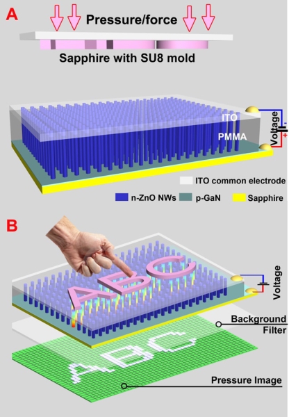
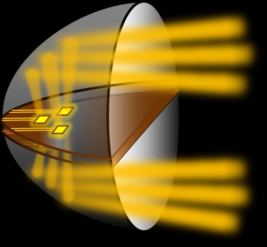
Piezo-phototronic LED schematic
Piezoelectric materials generate a charge polarization when they are placed under strain. The piezo-phototronic devices rely on that physical principle to tune and control the charge transport and recombination by the polarization charges present at the ends of individual nanowires. Grown atop a gallium nitride (GaN) film, the nanowires create pixeled light emitters whose output varies with the pressure, creating an electroluminescent signal that can be integrated with on-chip photonics for data transmission, processing and recording.
“When you have a zinc oxide nanowire under strain, you create a piezoelectric charge at both ends which forms a piezoelectric potential,” Wang explained. “The presence of the potential distorts the band structure in the wire, causing electrons to remain in the p-n junction longer and enhancing the efficiency of the LED.”
The efficiency increase in the LED is proportional to the strain created. Differences in the amount of strain applied translate to differences in light emitted from the root where the nanowires contact the gallium nitride film.
To fabricate the devices, a low-temperature chemical growth technique is used to create a patterned array of zinc oxide nanowires on a gallium nitride thin film substrate with the c-axis pointing upward. The interfaces between the nanowires and the gallium nitride film form the bottom surfaces of the nanowires. After infiltrating the space between nanowires with a PMMA thermoplastic, oxygen plasma is used to etch away the PMMA enough to expose the tops of the zinc oxide nanowires.
A nickel-gold electrode is then used to form ohmic contact with the bottom gallium-nitride film, and a transparent indium-tin oxide (ITO) film is deposited on the top of the array to serve as a common electrode.
When pressure is applied to the device through handwriting or other source of pressure, nanowires are compressed along their axial directions, creating a negative piezo-potential, while uncompressed nanowires have no potential.
The researchers have pressed letters into the top of the device, which produces a corresponding light output from the bottom of the device. This output – which can all be read at the same time – can be processed and transmitted.
The ability to see all of the emitters simultaneously allows the device to provide a quick response. “The response time is fast, and you can read a million pixels in a microsecond,” said Wang. “When the light emission is created, it can be detected immediately with the optical fiber.”
The nanowires stop emitting light when the pressure is relieved. Switching from one mode to the other takes 90 milliseconds or less, Wang said.
The researchers studied the stability and reproducibility of the sensor array by examining the light emitting intensity of the individual pixels under strain for 25 repetitive on-off cycles. They found that the output fluctuation was approximately five percent, much smaller than the overall level of the signal. The robustness of more than 20,000 pixels was studied.
A spatial resolution of 2.7 microns was recorded from the device samples tested so far. Wang believes the resolution could be improved by reducing the diameter of the nanowires – allowing more nanowires to be grown in a given space – and by using a high-temperature fabrication process.
In addition to Wang, the research team also included Caofeng Pan, Lin Dong, Guang Zhu, Simiao Niu, Ruomeng Yo, Qing Yang and Ying Liu, all associated with Georgia Tech. In addition, Pan is associated with the Beijing Institute of Nanoenergy and Nanosystems in the Chinese Academy of Sciences.
This research was supported by the U.S. Department of Energy (DOE), Office of Basic Energy Sciences, Division of Materials Sciences and Engineering under Award DE-FG02-07ER46394; the National Science Foundation (NSF) under award CMMI-040367; and by the Knowledge Innovation program of the Chinese Academy of Sciences under KJCX2-YW-M13. The opinions and conclusions expressed are those of the authors and do not necessarily represent the official views of the DOE or NSF.
CITATION: Caofeng Pan, et al., "High resolution electroluminescent imaging of pressure distribution using a piezoelectric nanowire-LED array," (Nature Photonics 2013). http://dx.doi.org/10.1038/nphoton.2013.191

