March 11, 2025
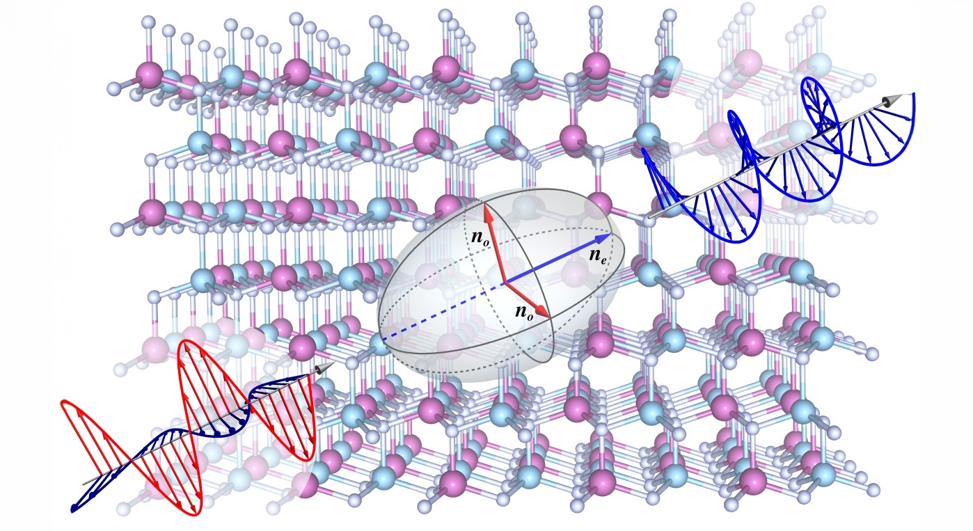
From integrated photonics to quantum information science, controlling light with electric fields — known as the electro-optic effect — is essential for applications such as light modulation and frequency transduction. These components rely on nonlinear optical materials, which enable precise manipulation of light waves through applying electric fields.
Conventional nonlinear optical materials such as lithium niobate have large electro-optic responses but are hard to integrate with silicon devices. In the search for silicon-compatible materials, aluminum scandium nitride (AlScN) has come to the fore. A1ScN is considered an excellent piezoelectric — able to generate electricity when pressure is applied or to deform when an electric field is applied. However, how to better control its properties and enhance its electro-optic coefficients has remained unanswered.
Now, researchers in Chris Van de Walle’s computational materials group at UC Santa Barbara have found a way to adjust the material’s atomic structure and composition to boost its performance. . Their study, published on the cover of Applied Physics Letters, explains how adjusting the material’s atomic structure and composition can boost its performance. A strong electro-optic response requires a large concentration of scandium — but the specific arrangement of the scandium atoms within the AlN crystal lattice matters.
“By using cutting-edge atomistic modeling, we found that placing scandium atoms in a regular array along a specific crystal axis greatly boosts the electro-optic performance,” explained Haochen Wang, the doctoral student who spearheaded the calculations.
This finding inspired the researchers to investigate so-called superlattice structures, in which atomically thin layers of ScN and AlN are alternately deposited, an approach that can be experimentally implemented using sophisticated growth techniques. They found that precisely oriented layer structures do indeed offer significant enhancements in electro-optic properties.
Intriguingly, the scientists also realized that strain can be exploited to tune the properties close to the “Goldilocks” point, where the largest electro-optic enhancements are obtained. Strain can result from externally applied stress, or it can be built into the material through carefully designed microstructures, now a routine approach in silicon technology. Careful strain tuning could yield an electro-optic effect in AlScN that is up to an order of magnitude greater than in lithium niobate, the current go-to material.
“We are excited about the potential of AlScN to push the boundaries of nonlinear optics,” said Van de Walle. “Equally importantly, the insights reaped from this study will allow us to systematically investigate other so-called heterostructural alloys that may feature even better performance.”
The research was supported by the Army Research Office and by SUPREME, a Semiconductor Research Corporation program sponsored by the Defense Advanced Research Projects Agency.


