May 27, 2024
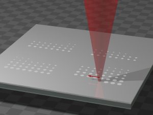
It was a serendipitous finding that led ARCNL/UvA PhD researcher Lorenzo Cruciani to the discovery of a new method to directly write patterns of ruthenium with a laser. In a recent paper in Applied Physics Letters, Cruciani and his colleagues describe their method that circumvents the use of photoresist in lithography processes.
In a project sponsored by the University of Amsterdam (UvA), Lorenzo Cruciani is studying laser-induced terahertz emission from layers of ruthenium. ‘One day, I accidentally exposed the ruthenium to a high laser power, and to my surprise, the amount of terahertz emission increased much more than expected.’ To check if anything weird happened to the substrate, the researcher removed the ruthenium with supermarket bleach. Where all of the unexposed ruthenium was dissolved as expected, the exposed part was not removed. Cruciani is a PhD student carrying out his research at ARCNL, under supervision of Paul Planken and Klaasjan van Druten.”
Heat-induced oxidation
One possible explanation for the observed effects was that the incident laser light had locally oxidized the surface of the ruthenium. A hunch that was further confirmed when Cruciani made a layer of ruthenium oxide on ruthenium on purpose and, after laser exposure, witnessed a similar enhancement of the terahertz radiation emission, as described in a previous publication of the group. Additional experiments and insights by his ARCNL colleagues Stefan van Vliet and Roland Bliem on the exposed sample indeed confirmed the presence of ruthenium oxide at its surface. In addition, a colleague of Lorenzo, Ester Abram, used a completely different laser to show that a very high power, single laser pulse was already sufficient to see hints of ruthenium oxidation and remnants of ruthenium at the surface after trying to dissolve the ruthenium in bleach.
The oxidation and thus the writing is the result of a thermal process, Paul Planken explains. ‘The energy from our pulsed laser at the center of the laser spot gives rise to a temperature that is high enough to locally oxidize the material.’
Shrinking spots
‘The next question was how small we could get,’ says Cruciani. By varying exposure parameters like the thickness of the ruthenium layer and the focus diameter and repetition rate of the laser, the researcher managed to bring down the size of the islands he could write from 18 to 9 micrometer. With the aid of Dries van Oosten and Marnix Vreugdenhil from Utrecht University and their dedicated equipment, islands with diameters as small as 500 nanometers were produced. ‘Since we were working with a laser spot of 2 microns, this means that we managed to write structures that are four times smaller than the diffraction limit,’ stresses Planken.
Explore the limits
Ruthenium is of interest for the semiconductor industry to possibly replace commonly used materials like copper, which at the nanoscale become less conductive. Since the new laser writing method circumvents the use of photoresist and thus requires fewer and less cumbersome processing steps, the researchers are eager to further explore the limits of the technique, Cruciani and Planken say.
‘There are so many things we can start looking at now. We can for example play around with the laser: use different sources, vary the number of laser pulses, change the time in between subsequent pulses, … And we can look at entirely different writing concepts. For example, at the moment, we are writing the patterns with a focused beam. But perhaps we could also use a wide beam and a mask to write multiple structures at once. The fun thing about this method is that we are using a widely known, classical thermal effect to write things that are really small. This paper might very well mark the starting point of an entirely new angle to printing small patterns in ruthenium.’
Reference
Lorenzo Cruciani, Marnix Vreugdenhil, Stefan van Vliet, Ester Abram, Dries van Oosten, Roland Bliem, Klaasjan van Druten, and Paul Planken, Direct laser patterning of ruthenium below the optical diffraction limit, Appl. Phys. Lett. 124, 171902 (2024).
https://doi.org/10.1063/5.0205538


