
2024.05.08
- World's first confirmation of a unique phenomenon combining optical, electrical, and mechanical properties when light is fired at a 2D atomic layer... Can be applied as a 2D nano actuator moving with light
- GIST-University of Pennsylvania joint research team published a paper in the international journal <Nano Letters>
The results of observation and analysis of a phenomenon that combines optical, electrical, and mechanical properties in a two-dimensional atomic layer were revealed by a joint Korean-American research team.
The Gwangju Institute of Science and Technology (GIST, President Kichul Lim) announced that a team of researchers led by Senior Researcher Sang-Youp Yim of the Advanced Photonics Research Institute and collaborators from the University of Pennsylvania in the United States have identified polarons* as the cause of the phenomenon that causes thin films to swell and locally change semiconductor doping properties when light is shone on a two-dimensional atomic layer.
Two-dimensional semiconductor materials*, which utilize two-dimensional nanomaterials instead of silicon, are promising future materials because of their unique electrical, optical, chemical, and mechanical properties, but the phenomenon of how these properties are combined is not yet clearly understood.
One of these phenomena is photocompression (or photodilation), which is the change in size or shape of a sample when light is shone on it without applying heat. If photocompression or photodilation occurs in a two-dimensional layer of atoms, it is possible to develop nanosystems that can control mechanical motion at the nanometer scale.
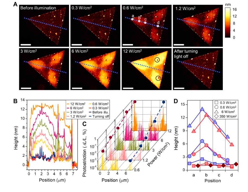
Expansion of the WS2 atomic layer depending on the intensity of light. As a result of observing the change in surface height while injecting a red laser beam into the WS2 atomic layer, a reversible expansion phenomenon was observed depending on the intensity of light. Similar results were obtained with a blue laser beam that can be absorbed by the WS2 atomic layer, but there was no change with a near-infrared laser beam without absorption.
Credit: GIST
As a result of observing the change in surface height with an atomic force microscope by applying a red laser beam to the tungsten disulfide (WS2) atomic layer, it was observed that the area with few defects began to swell first, resulting in a symmetrical expansion pattern. It was confirmed that this is a reversible phenomenon in which it expands significantly as the intensity of light increases, and returns to its original state when no light is applied. A similar phenomenon was observed when using a blue laser instead of a red laser.
However, the near-infrared laser, which is not absorbed by the tungsten disulfide (WS2) atomic layer, showed no change even when fired at very high intensity. It was confirmed that charge carriers and defects* excited* by absorbed light play an important role.
The research team observed with a Kelvin microscope* that the semiconductor doping characteristics change in a local area depending on the intensity of light and a local p-n junction occurs. As a result, it was found that the electron-polaron state bound to the defect is the cause of lattice expansion and local change in semiconductor doping characteristics.
The research team discovered that when light shines on the atomic layer of tungsten disulfide (WS2), a type of transition metal dichalcogenide twodimensional semiconductor thin film, the thin film swells into a patterned shape and the semiconductor doping characteristics change in a local region, forming a local p-n junction*. This phenomenon was observed, and it was revealed that electron-polarons were the cause.
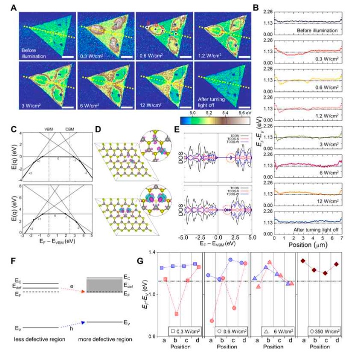
Change in the semiconductor doping characteristics of the WS2 atomic layer depending on the intensity of light. Observation of the phenomenon in which the semiconductor doping characteristics change in a local region and a local p-n junction occurs. Electronic calculations confirmed that the cause of lattice expansion and local change in semiconductor doping characteristics was electron-polaron bound to defects.
Credit: GIST
The observation and analysis of a phenomenon that combines optical, electrical, and mechanical properties in a two-dimensional atomic layer is the world's first research result reported by the research team.
Senior Researcher Sang-Youp Yim said, "This research will serve as a cornerstone of attempts to observe similar phenomena in various 2D semiconductor materials and to control the type/density of defects. It is expected that it will be possible to develop optical-nano actuators that are ultra-small and operate at low power in the future."
This research, conducted in collaboration with Senior Researcher Sang-Youp Yim's team at the GIST Advanced Photonics Research Institute and Professor Agarwal's team and Professor Rappe's team at the University of Pennsylvania, was supported by the National Research Foundation of Korea's Basic Research Project in Science and Engineering and the GIST Advanced Photonics Research Institute's own project. It was published online in 'Nano Letters' on April 24, 2024.
* Polaron: A quasiparticle concept introduced to understand the interaction between charge carriers and atoms in solid materials. Charge carriers such as electrons and holes can interact with lattice vibrations and cause lattice deformation. Instead of thinking of this phenomenon as a reaction between charge carriers and atoms (lattice strain), the concept is to view charge carriers as quasiparticles that move while ‘wearing’ lattice strain.
* 2D semiconductor materials: 2D materials are materials with a thickness of one atomic layer, such as graphene, and are expected to replace silicon materials. However, compared to silicon semiconductors, it is difficult to control the electrical characteristics, so it is difficult to implement the desired logic device.
* excitation: When the electrons in the outermost shell of an atom are given energy from the outside, they move to an electron orbit with a high energy level. An atom or molecule in this state is said to be in an excited state.
* defect: A solid with a crystal structure is formed by a periodic arrangement of atoms, but the regularity is not always perfect and broken areas exist, which are referred to as defects. It can be classified into point, line, surface, and volume defects, and various defects are formed depending on the location, direction, and type of atoms.
* p-n junction: The basic structure of a diode that allows current to flow in only one direction when an external voltage is applied when joining a p-type semiconductor and an n-type semiconductor.
* Kelvin microscope (Scanning Kelvin-probe Force Microscopy): A type of atomic force microscope using a technique that locally measures/images the work function of a material by detecting the electrostatic force between the probe and the sample. For semiconductor materials, semiconductor doping characteristics can be quantitatively measured.


