June 15, 2023
What’s New: Today, Intel announced the release of its newest quantum research chip, Tunnel Falls, a 12-qubit silicon chip, and it is making the chip available to the quantum research community. In addition, Intel is collaborating with the Laboratory for Physical Sciences (LPS) at the University of Maryland, College Park’s Qubit Collaboratory (LQC), a national-level Quantum Information Sciences (QIS) Research Center, to advance quantum computing research.
Why It Matters: Currently, academic institutions don’t have high-volume manufacturing fabrication equipment like Intel. With Tunnel Falls, researchers can immediately begin working on experiments and research instead of trying to fabricate their own devices. As a result, a wider range of experiments become possible, including learning more about the fundamentals of qubits and quantum dots and developing new techniques for working with devices with multiple qubits.
To further address this, Intel is collaborating with LQC as part of the Qubits for Computing Foundry (QCF) program through the U.S. Army Research Office to provide Intel’s new quantum chip to research laboratories. The collaboration with LQC will help democratize silicon spin qubits by enabling researchers to gain hands-on experience working with scaled arrays of these qubits. The initiative aims to strengthen workforce development, open the doors to new quantum research and grow the overall quantum ecosystem.
The first quantum labs to participate in the program include LPS, Sandia National Laboratories, the University of Rochester, and the University of Wisconsin-Madison. LQC will work alongside Intel to make Tunnel Falls available to additional universities and research labs. The information gathered from these experiments will be shared with the community to advance quantum research and to help Intel improve qubit performance and scalability.
“The LPS Qubit Collaboratory, in partnership with the Army Research Office, seeks to tackle the hard challenges facing qubit development and develop the next generation of scientists who will create the qubits of tomorrow,” said Charles Tahan, chief of Quantum Information Science, LPS. “Intel’s participation is a major milestone to democratizing the exploration of spin qubits and their promise for quantum information processing and exemplifies LQC’s mission to bring industry, academia, national labs, and government together.”
Dr. Dwight Luhman, distinguished member of Technical Staff at Sandia National Laboratories, said, “Sandia National Laboratories is excited to be a recipient of the Tunnel Falls chip. The device is a flexible platform enabling quantum researchers at Sandia to directly compare different qubit encodings and develop new qubit operation modes, which was not possible for us previously. This level of sophistication allows us to innovate novel quantum operations and algorithms in the multi-qubit regime and accelerate our learning rate in silicon-based quantum systems. The anticipated reliability of Tunnel Falls will also allow Sandia to rapidly onboard and train new staff working in silicon qubit technologies.“
Mark A. Eriksson, department chair and John Bardeen Professor of Physics, Department of Physics, University of Wisconsin-Madison, said, “UW-Madison researchers, with two decades of investment in the development of silicon qubits, are very excited to partner in the launch of the LQC. The opportunity for students to work with industrial devices, which benefit from Intel’s microelectronics expertise and infrastructure, opens important opportunities both for technical advances and for education and workforce development.”
A photo shows the Intel Tunnel Falls chip in packaging. Tunnel Falls is the first silicon spin qubit device released to research institutes and universities. It is fabricated on 300-millimeter wafers and leverages Intel’s most advanced transistor fabrication capabilities. (Credit: Intel Corporation)
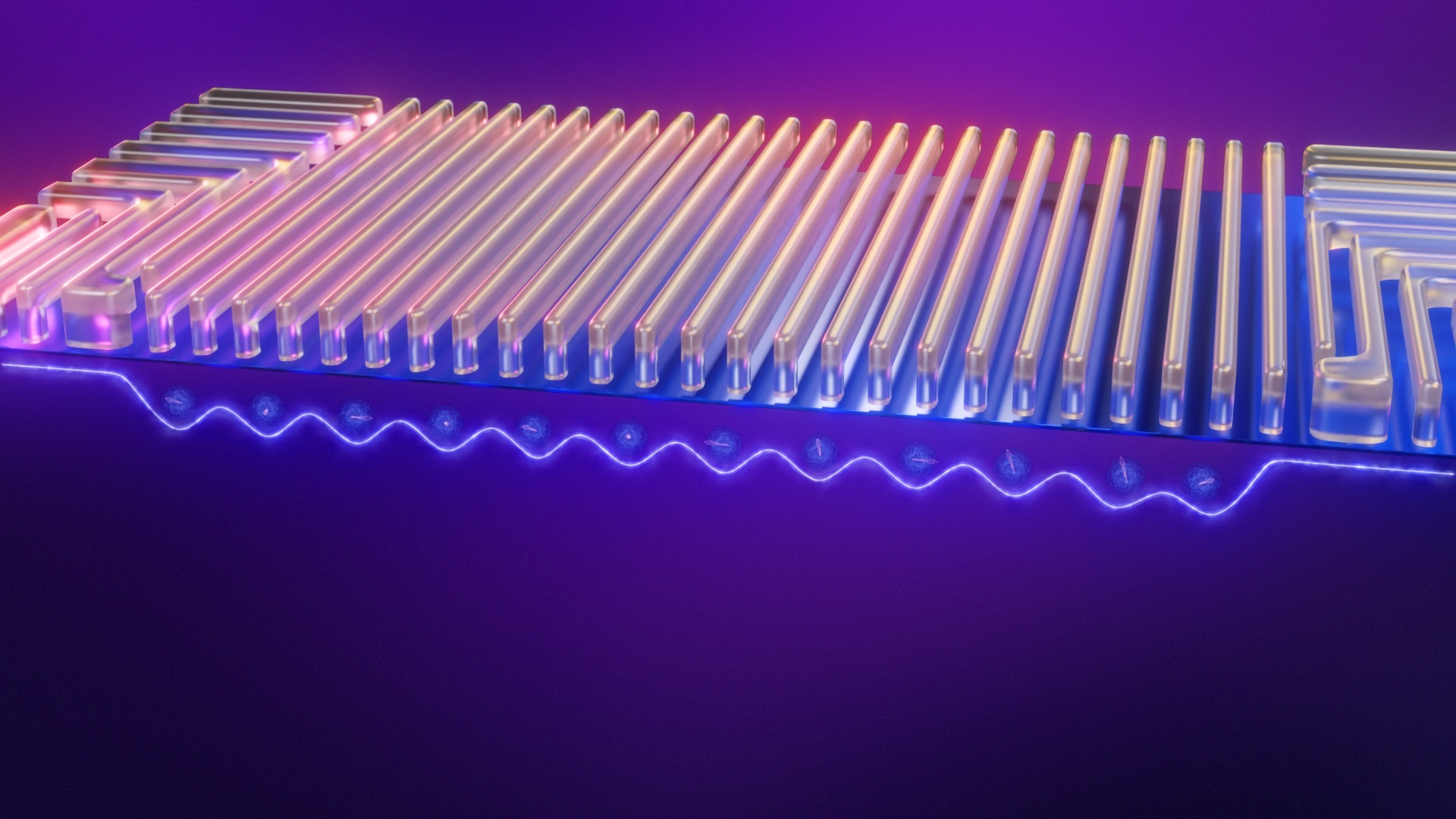
About Tunnel Falls: Tunnel Falls is Intel’s first silicon spin qubit device released to the research community. Fabricated on 300-millimeter wafers in the D1 fabrication facility, the 12-qubit device leverages Intel’s most advanced transistor industrial fabrication capabilities, such as extreme ultraviolet lithography (EUV) and gate and contact processing techniques. In silicon spin qubits, information (the 0/1) is encoded in the spin (up/down) of a single electron. Each qubit device is essentially a single electron transistor, which allows Intel to fabricate it using a similar flow to that used in a standard complementary metal oxide semiconductor (CMOS) logic processing line.
Intel believes silicon spin qubits are superior to other qubit technologies because of their synergy with leading-edge transistors. Being the size of a transistor, they are up to 1 million times smaller than other qubit types measuring approximately 50 nanometers by 50 nanometers, potentially allowing for efficient scaling. According to Nature Electronics, “Silicon may be the platform with the greatest potential to deliver scaled-up quantum computing.”
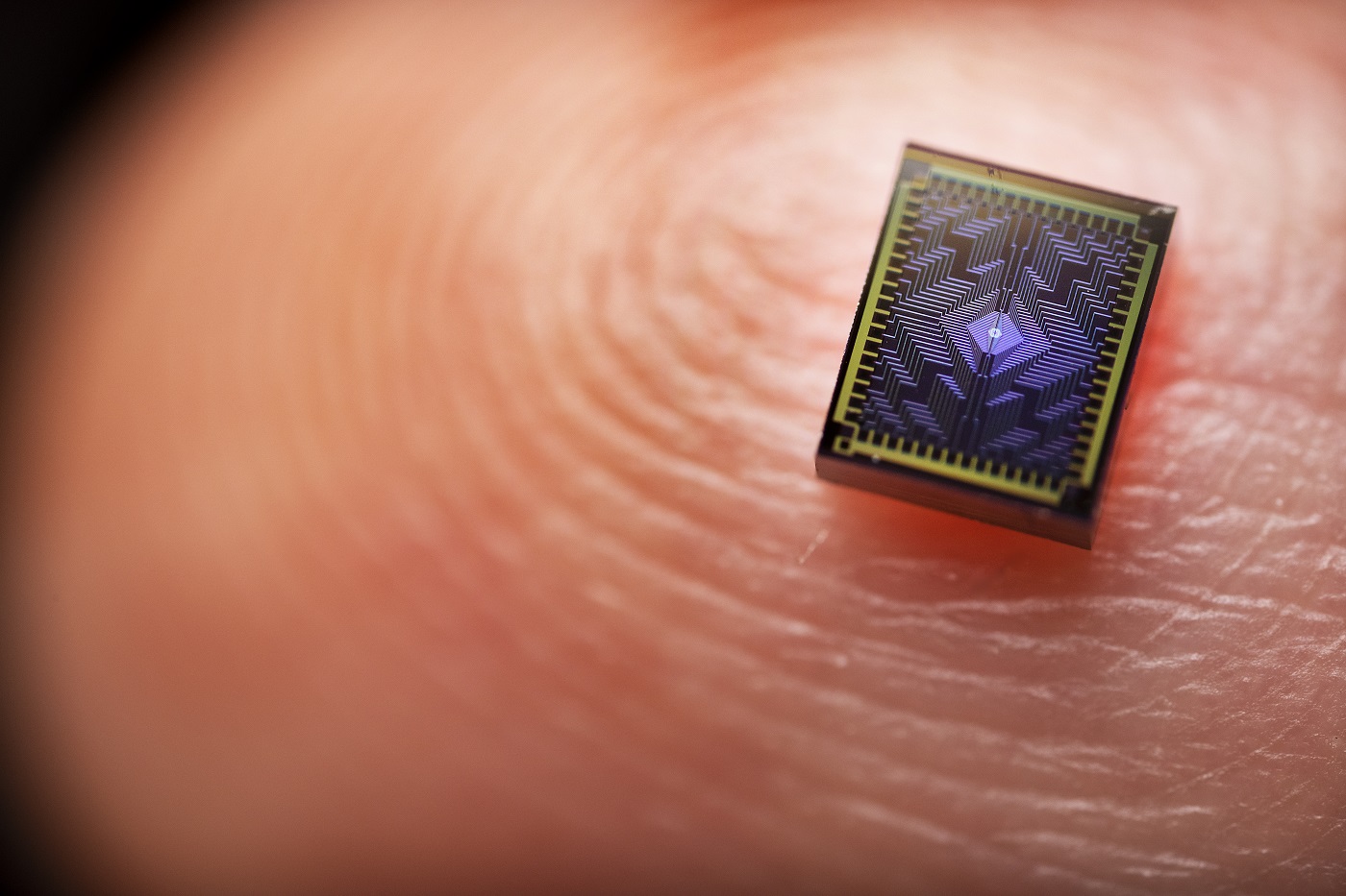
A photo shows one of Intel's Tunnel Falls chips on a human finger to display its scale. Silicon spin qubits are up to 1 million times smaller than other qubit types. The Tunnel Falls chip measures approximately 50-nanometers square, potentially allowing for faster scaling. (Credit: Intel Corporation)
At the same time, utilizing advanced CMOS fabrication lines allows Intel to use innovative process control techniques to enable yield and performance. For example, the Tunnel Falls 12 qubit device has a 95% yield rate across the wafer and voltage uniformity similar to a CMOS logic process, and each wafer provides over 24,000 quantum dot devices. These 12-dot chips can form between four to 12 qubits that can be isolated and used in operations simultaneously depending on how the university or lab operates its systems.

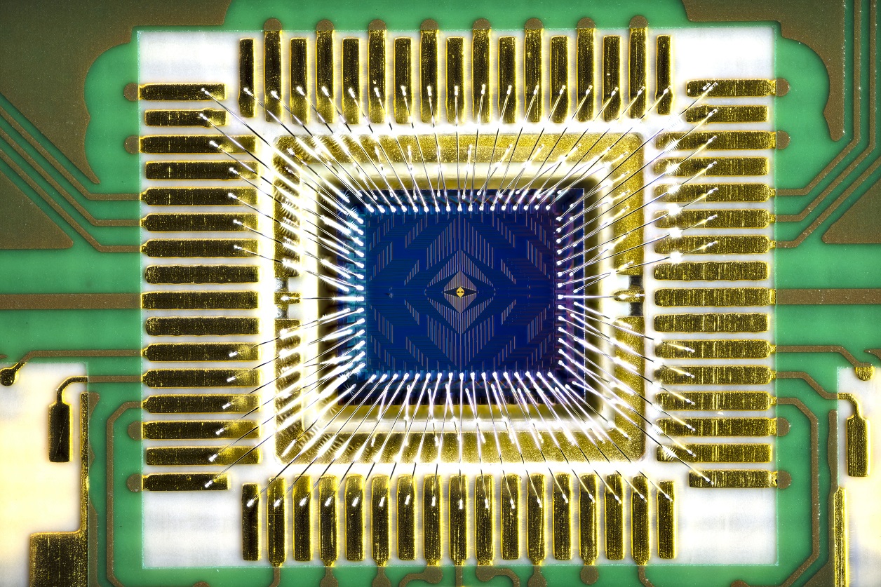
A photo shows a magnified view of Intel's Tunnel Falls chip. Tunnel Falls provides a 95% yield rate across the wafer and voltage uniformity similar to a CMOS logic process. A wafer provides 24,000 quantum dot test chips with a 99.8% yield tuned at the single electron level. These 12-dot chips can form between four to 12 qubits that can be isolated and used in operations simultaneously depending on how a university or lab operates its systems. (Credit: Intel Corporation)
What’s Next: Intel will continuously work to improve the performance of Tunnel Falls and integrate it into its full quantum stack with the Intel Quantum Software Development Kit (SDK). In addition, Intel is already developing its next-generation quantum chip based on Tunnel Falls; it is expected to be released in 2024. In the future, Intel plans to partner with additional research institutions globally to build the quantum ecosystem.


