June 24, 2022
By Amanda Siegfried
University of Texas at Dallas physicists and their collaborators at Yale University have demonstrated an atomically thin, intelligent quantum sensor that can simultaneously detect all the fundamental properties of an incoming light wave.
The research, published April 13 in the journal Nature, demonstrates a new concept based on quantum geometry that could find use in health care, deep-space exploration and remote-sensing applications.
“We are excited about this work because typically, when you want to characterize a wave of light, you have to use different instruments to gather information, such as the intensity, wavelength and polarization state of the light. Those instruments are bulky and can occupy a significant area on an optical table,” said Dr. Fan Zhang, a corresponding author of the study and associate professor of physics in the School of Natural Sciences and Mathematics.
“Now we have a single device — just a tiny and thin chip — that can determine all these properties simultaneously in a very short time,” he said.

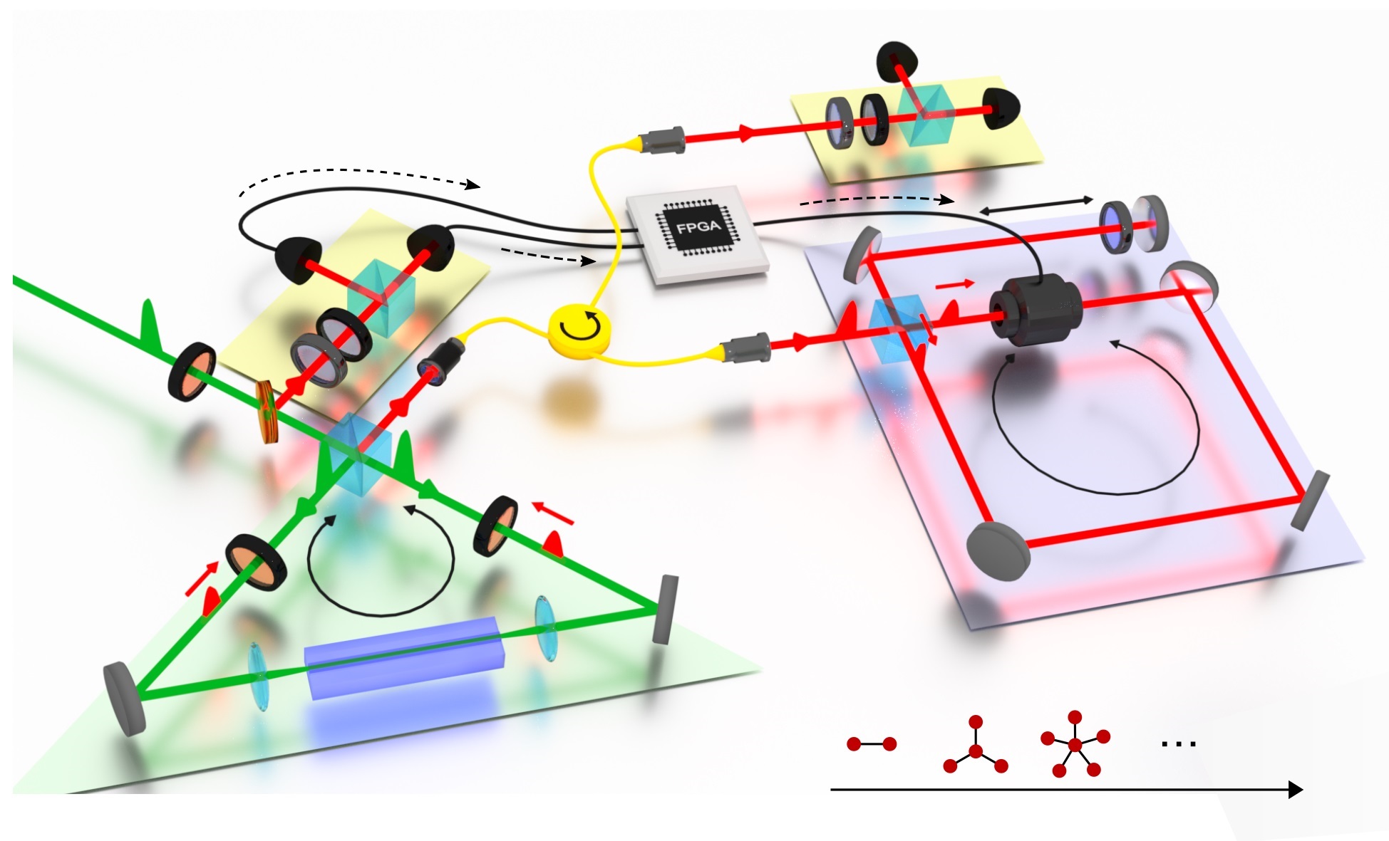
This artistic rendering depicts the intelligent sensing process of two-dimensional materials called moiré metamaterials. Quantum geometric properties of the metamaterial determine how it responds to an incoming light wave. The wave’s fundamental properties are then interpreted by a neural network. (Image courtesy of Dr. Fengnian Xia, Yale University)
The device exploits the unique physical properties of a novel family of two-dimensional materials called moiré metamaterials. Zhang, a theoretical physicist, published a review article on these materials Feb. 2 in Nature.
The 2D materials have periodic structures and are atomically thin. If two layers of such a material are overlaid with a small rotational twist, a moiré pattern with an emergent, orders-of-magnitude larger periodicity can form. The resulting moiré metamaterial yields electronic properties that differ significantly from those exhibited by a single layer alone or by two naturally aligned layers.
The sensing device that Zhang and his colleagues chose to demonstrate their new idea incorporates two layers of relatively twisted, naturally occurring bilayer graphene, for a total of four atomic layers.
“The moiré metamaterial exhibits what’s called a bulk photovoltaic effect, which is unusual,” said Patrick Cheung, a physics doctoral student at UT Dallas and co-lead author of the study. “Normally, you have to apply a voltage bias to produce any current in a material. But here, there is no bias at all; we simply shine a light on the moiré metamaterial, and the light generates a current via this bulk photovoltaic effect. Both the magnitude and phase of the photovoltage are strongly dependent on the light intensity, wavelength and polarization state.”
By tuning the moiré metamaterial, the photovoltage generated by a given incoming light wave creates a 2D map that is unique to that wave — like a fingerprint — and from which the wave’s properties might be inferred, although doing so is challenging, Zhang said.
Researchers in Dr. Fengnian Xia’s lab at Yale University, who constructed and tested the device, placed two metal plates, or gates, on top and underneath the moiré metamaterial. The two gates allowed the researchers to tune the quantum geometric properties of the material to encode the infrared light waves’ properties into “fingerprints.”
The team then used a convolutional neural network — an artificial intelligence algorithm that is widely used for image recognition — to decode the fingerprints.
“We start with light for which we know the intensity, wavelength and polarization, shine it through the device and tune it in different ways to generate different fingerprints,” Cheung said. “After training the neural network with a data set of about 10,000 examples, the network is able to recognize the patterns associated with these fingerprints. Once it learns enough, it can characterize an unknown light.”
Cheung performed theoretical calculations and analysis using the resources of the Texas Advanced Computing Center, a supercomputer facility on the UT Austin campus.
“Patrick has been good at pencil-and-paper analytical calculations — that is my style — but now he has become an expert in using a supercomputer, which is required for this work,” Zhang said. “On the one hand, our job as researchers is to discover new science. On the other hand, we advisors want to help our students discover what they are best at. I’m very happy that Patrick and I figured out both.”
In addition to the Yale researchers, other authors included scientists from the National Institute for Materials Science in Japan.
Funding for the UTD researchers involved in this work came from the National Science Foundation and the Army Research Office, a component of the U.S. Army Combat Capabilities Development Command Army Research Laboratory.

