November 17, 2022
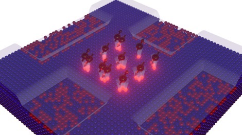
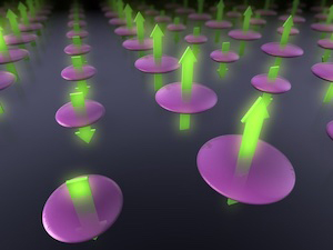
Researchers at the National Institute of Standards and Technology (NIST) have created grids of tiny clumps of atoms known as quantum dots and studied what happens when electrons dive into these archipelagos of atomic islands. Measuring the behavior of electrons in these relatively simple setups promises deep insights into how electrons behave in complex real-world materials and could help researchers engineer devices that make possible powerful quantum computers and other innovative technologies.
In work published in Nature Communications, the researchers made multiple 3-by-3 grids of precisely spaced quantum dots, each comprising one to three phosphorus atoms. Attached to the grids were electrical leads and other components that enabled electrons to flow through them. The grids provided playing fields in which electrons could behave in nearly ideal, textbook-like conditions, free of the confounding effects of real-world materials.
The researchers injected electrons into the grids and observed how they behaved as the researchers varied conditions such as the spacing between the dots. For grids in which the dots were close, the electrons tended to spread out and act like waves, essentially existing in several places at one time. When the dots were far apart, they would sometimes get trapped in individual dots, like electrons in materials with insulating properties.
The grids provided playing fields in which electrons could behave in nearly ideal, textbook-like conditions, free of the confounding effects of real-world materials.
Advanced versions of the grid would allow researchers to study the behavior of electrons in controllable environments with a level of detail that would be impossible for the world’s most powerful conventional computers to simulate accurately. It would open the door to full-fledged “analog quantum simulators” that unlock the secrets of exotic materials such as high-temperature superconductors. It could also provide hints about how to create materials, such as topological insulators, by controlling the geometry of the quantum dot array.
In related work just published in ACS Nano, the same NIST researchers improved their fabrication method so they can now reliably create an array of identical, equally spaced dots with exactly one atom each, leading to even more ideal environments necessary for a fully accurate quantum simulator. The researchers have set their sights on making such a simulator with a larger grid of quantum dots: A 5x5 array of dots can produce rich electron behavior that is impossible to simulate in even the most advanced supercomputers.
Papers:
Xiqiao Wang, Ehsan Khatami, Fan Fei, Jonathan Wyrick, Pradeep Namboodiri, Ranjit Kashid, Albert F. Rigosi, Garnett Bryant and Richard M. Silver. Experimental Realization of an Extended Fermi-Hubbard Model Using a 2D Lattice of Dopant-based Quantum Dots. Nature Communications. Published online Nov. 11, 2022. DOI: 10.1038/s41467-022-34220-w
Jonathan Wyrick, Xiqiao Wang, Pradeep Namboodiri, Ranjit V. Kashid, Fan Fei, Joseph Fox and Richard M. Silver. Enhanced Atomic Precision Fabrication by Adsorption of Phosphine into Engineered Dangling Bonds on H-Si Using STM and DFT. ACS Nano. Published online Nov. 2, 2022. DOI: 10.1021/acsnano.2c08162

