December 5, 2022
By Harrison Tasoff
Photonics. It’s a word to know. This technology uses light instead of electricity. It’s fast; it’s versatile; and it’s poised to be the next major advancement in human technology.
So far, photonics research has required expensive, sophisticated equipment like precision lasers and custom circuitry. But to realize its full potential, the technology has to get a lot smaller, cheaper and easier to produce. Researchers have made progress on these fronts, but still face challenges getting their circuits to work with shorter wavelengths of light.
In a finding that promises to make these components smaller and more powerful, a team from Nexus Photonics, UC Santa Barbara and Caltech has developed a technique to enable photonic chips to operate in the visible-to-near-infrared spectrum. The technique also takes advantage of methods common in electronic manufacturing, making it easy to produce inexpensively at scale. The results appear in the journal Nature.
“This is the kind of breakthrough that could open up possibilities no one has thought of before,” said co-lead author Ted Morin, a doctoral candidate at UC Santa Barbara. The technology will take high-performance photonics into new markets and applications, such as augmented and virtual reality, healthcare and atomic clocks at visible and near-infrared wavelengths. What’s more, large-scale production will slash the price of lasers and photonic circuits. “It will be like getting a yacht for the cost of a surfboard,” Morin said.
Society’s progress over the last half century has followed the progress of electronics, which have gotten ever smaller and more powerful. “Humanity has collectively done an amazing job of making smaller, faster, more reliable electronic circuits,” Morin said. “We’re figuring out ways to use the manufacturing technology for electronic circuits to make photonic circuits.”
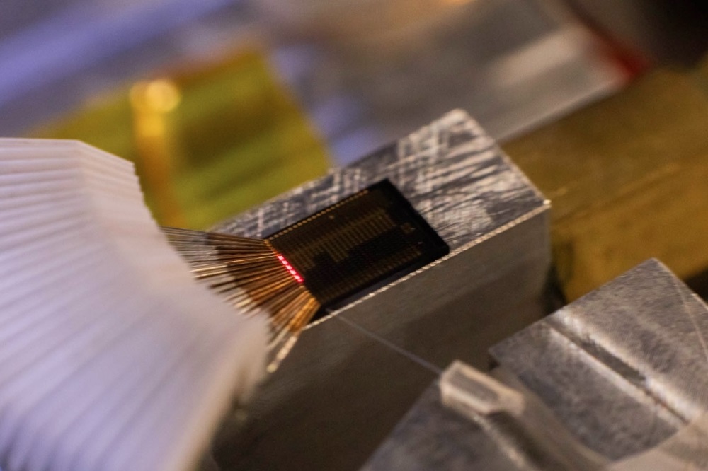
Light information and energy transmit through waveguides in a photonic circuit, much like electricity in the wires of an electronic circuit. A huge hurdle to miniaturization has been connecting the laser to the photonic circuit itself. But plugging it into each pathway simply isn’t practical. “Imagine someone plugging wires in, by hand, to every few transistors on your computer processor,” Morin said.
“It would completely defeat the purpose of making things more compact,” added co-lead author Minh Tran, the research director at Nexus Photonics, who earned his doctorate at UC Santa Barbara.
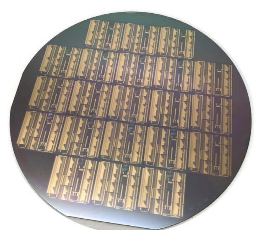
This fully processed, 4-inch wafer contains thousands of devices.
Photo Credit: MINH TRAN ET AL.
This “laser connection” problem was elegantly solved for silicon circuitry in 2005 by researchers at UC Santa Barbara, led by Professor John Bowers. They overcame this hurdle by bonding the laser materials right on top of the silicon and bending the light down into the waveguides. That technology and its variation have since been developed by multiple industrial and research institutes, and commercialized by Intel at multimillion dollar per annum scale.
Unfortunately, these solutions come with a catch. They only work for light with a wavelength longer than 1,100 nanometers, which is deep within the infrared. Every semiconductor has what’s called a “band gap energy,” and photons with a higher energy (i.e., smaller wavelength) than this are absorbed by the material. Silicon’s bandgap is around 1,100 nm. “So whatever is shorter than that doesn’t work with the current technology,” Tran said. Visible light ranges from 380 to 750 nm, meaning that UV, visible light and even some infrared is absorbed by silicon waveguides.
So, while silicon is great for electronics, it can’t transmit light at every wavelength that scientists and engineers want. “If we want to extend our applications to shorter wavelengths, we need to use a different material to guide our light,” Tran explained.
Silicon nitride emerged as the best candidate. The material’s bandgap is about 250 nm, well into the ultraviolet part of the spectrum. And since it’s a silicon compound, it easily integrates with electronic manufacturing practices. Its components, silicon and nitrogen, are also plentiful and inexpensive. “Elementally, it’s sand plus air,” Morin said. And the entire process involves routine manufacturing steps and can easily be scaled up with existing infrastructure.
But now the challenge of connecting lasers to waveguides had to be addressed again, since the original technique on silicon doesn’t work with silicon nitride due to its optical properties. Light travels at different speeds depending on the substance it’s passing through. Scientists describe the speed of light in a material with a number called a refractive index, and silicon nitride has a very different index than the laser material. This makes it difficult to bend the beam of light from the laser layer into the silicon nitride waveguides below it.
To address this issue, the team added an intermediary material with a refractive index close to that of silicon nitride on the same plane as the laser. This way, the laser light could enter the transitional waveguide head-on and then be directed down into the silicon nitride from a material with similar optical properties. And while design was a step forward, the true challenge was making the process compatible with standard electronic manufacturing processes, Tran explained.
The achievement marks a major breakthrough for the team. “In 2018, several of us from UCSB founded Nexus Photonics to solve the challenge of making short-wavelength photonic integrated circuits,” said co-founder and CEO Tin Komljenovic. “Now we have finally optimized the technology to the point where it exceeds the performance of large commercial systems while being smaller than a dime.”
“This is an important milestone in the semiconductor and photonic field,” added UC Santa Barbara graduate and co-lead author Chong Zhang, co-founder and vice president of engineering at Nexus Photonics. “It provides a feasible and scalable solution, for the first time, for the full photonic integration in the visible-to-near-infrared wavelength.”
The laser-coupling technique will make high-powered, precision photonics orders of magnitude less expensive. As a result, they will be accessible for researchers making discoveries, for engineers making better technology, and eventually even for consumer electronics. After all, mass-produced, miniaturized photonic circuits are exactly the kind of components that can be incorporated into consumer goods.
There are all kinds of applications, the authors explained. This technology may find its way into biomedical sciences through applications like biosensing and DNA sequencing. It will certainly open up new avenues in atomic physics and quantum research. “The use of commercial silicon foundries is going to mean every university professor at every school in the world will be able to afford equipment and perform experiments that are now only feasible at major research institutions,” Morin said.
“We’re democratizing access to quantum physics,” Tran added.
Photonics could also revolutionize virtual and augmented reality. “With integrated photonics, it is possible to take light from a small chip and send it in a precisely controlled direction,” Morin said. “Sweeping the direction quickly, you can project images dynamically.
“You can also detect where light is coming from on the same chip,” he continued. “So it is possible to shine a light somewhere and see what comes back all in one tiny package.” That’s the idea behind lidar, the laser equivalent to radar, which is revolutionizing our driving experience.
The team has successfully integrated photonics into the electronic manufacturing sector, and they’re already looking at their next challenge. Eventually, they plan integrate photonic and electronic circuits onto the same chip, achieving even greater efficiencies in cost and capability.


