November 17, 2022
WRITTEN BY Robert Perkins
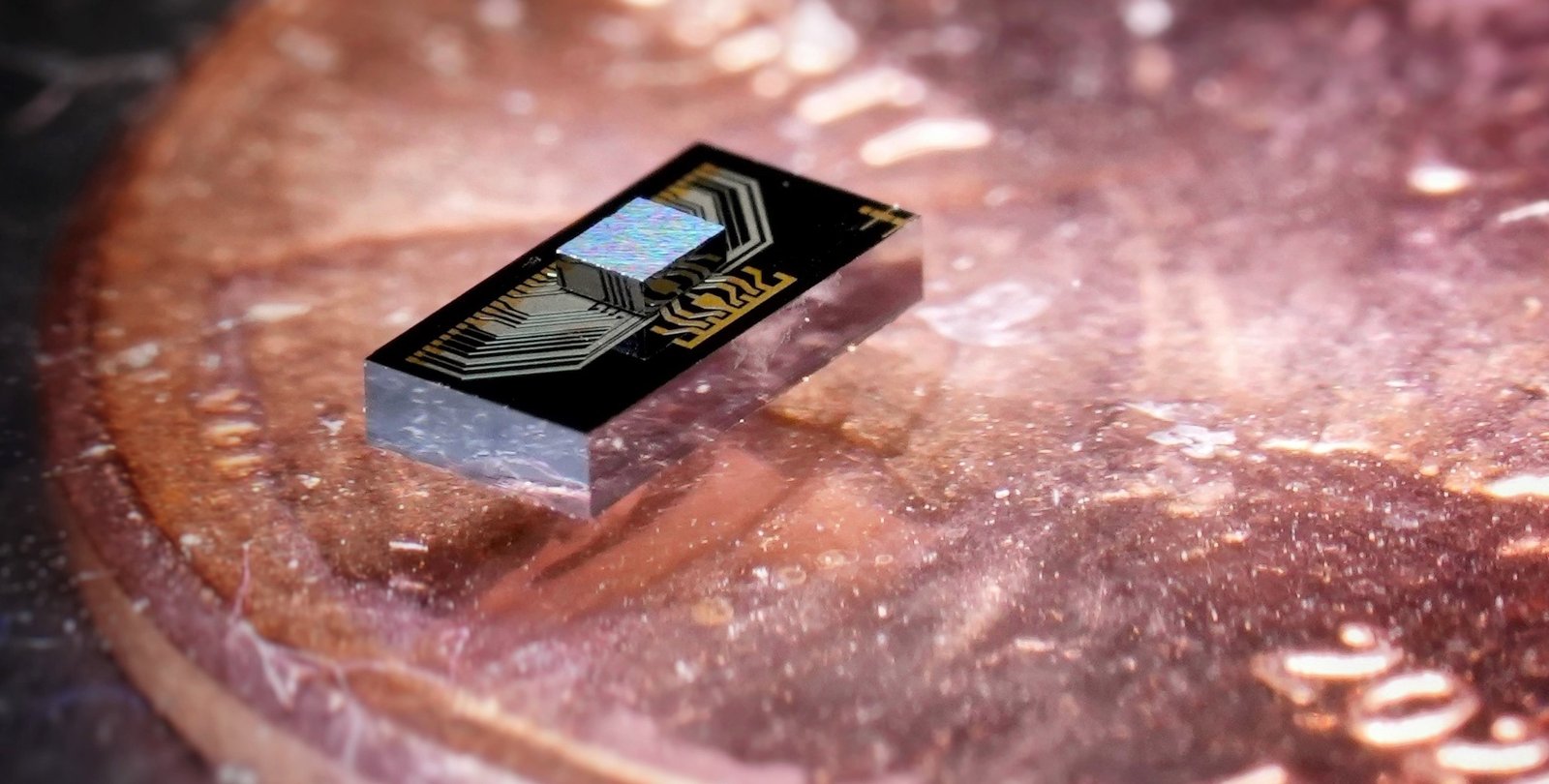
Engineers at Caltech and the University of Southampton in England have collaboratively designed an electronics chip integrated with a photonics chip (which uses light to transfer data)—creating a cohesive final product capable of transmitting information at ultrahigh speed while generating minimal heat.
Though the two-chip sandwich is unlikely to find its way into your laptop, the new design could influence the future of data centers that manage very high volumes of data communication.
"Every time you are on a video call, stream a movie, or play an online video game, you're routing data back and forth through a data center to be processed," says Caltech graduate student Arian Hashemi Talkhooncheh (MS '16), lead author of a paper describing the two-chip innovation that was published in the IEEE Journal of Solid-State Circuits on November 3. "There are more than 2,700 data centers in the U.S. and more than 8,000 worldwide, with towers of servers stacked on top of each other to manage the load of thousands of terabytes of data going in and out every second."
Just as your laptop heats up on your lap while you use it, the towers of servers in data centers that keep us all connected also heat up as they work, just at a much greater scale. Some data centers are even built underwater to cool whole facility more easily. The more efficient they can be made, the less heat they will generate, and ultimately, the greater the volume of information that they will be able to manage.
Data processing is done on electronic circuits, while data transmission is most efficiently done using photonics. Achieving ultrahigh speed in each domain is very challenging, but engineering the interface between them is even more difficult.
"There is a continuous demand for increasing the speed of data communication between different chips not only in data centers but also in high-performance computers. As the computing power of the chips scale, the communication speed can become the bottleneck, especially under stringent energy constraints," says Azita Emami, the Andrew and Peggy Cherng Professor of Electrical Engineering and Medical Engineering; executive officer for electrical engineering; and senior author of the paper.
To address this challenge, the Caltech/Southampton team designed both an electronics chip and a photonics chip from the ground up and co-optimized them to work together. The process, from the initial idea to the final test in the lab, took four years to complete, with every design choice impacting both chips.
"We had to optimize the entire system all at the same time, which enabled achieving a superior power efficiency," Hashemi says. "These two chips are literally made for each other, integrated into one another in three dimensions."
The resulting optimized interface between the two chips allows them to transmit 100 gigabits of data per second while producing just 2.4 pico-Joules per transmitted bit. This improves the electro-optical power efficiency of the transmission by a factor of 3.6 compared to the current state-of-the-art. A picojoule is one-trillionth of a Joule, which is defined as the energy released in one second by a current of 1 ampere through a resistance of 1 ohm—or about 0.24 calories.
"As the world becomes more and more connected, and every device generates more data, it is exciting to show that we can achieve such high data rates while burning a fraction of power compared to the traditional techniques," says Emami.
The paper is titled "A 100Gb/s PAM4 Optical Transmitter in A 3D-Integrated SiPh-CMOS Platform Using Segmented MOSCAP Modulators." Co-authors include Caltech graduate student Minwo Wang (MS '18) as well as Weiwei Zhang, David J. Thomson, Martin Ebert, Li Ke, and Graham T. Reed of the University of Southampton. This research was funded by Rockley Photonics and the U.K. Engineering and Physical Sciences Research Council.


