February 9, 2021
By James Badham
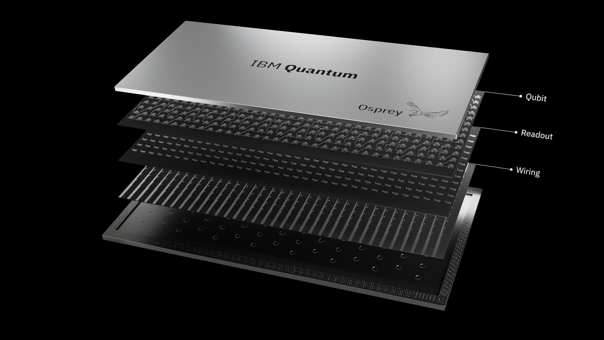
Classical computing is built on the power of the bit, which is, in essence, a micro transistor on a chip that can be either on or off, representing a 1 or a 0 in binary code. The quantum computing equivalent is the qubit. Unlike bits, qubits can exist in more than one “state” at a time, enabling quantum computers to perform computational functions exponentially faster than can classical computers.
To date, most efforts to build quantum computers have relied on qubits created in superconducting wires chilled to near absolute zero or on trapped ions held in place by lasers. But those approaches face certain challenges, most notably that the qubits are highly sensitive to environmental factors. As the number of qubits increases, those factors are more likely to compound and interrupt the entanglement of qubits required for a quantum computer to work.
Another approach, developed more recently, is to use a photon as an optical qubit to encode quantum information and to integrate the components necessary for that process into a photonic integrated circuit (PIC). Galan Moody, an assistant professor in the UC Santa Barbara College of Engineering’s Department of Electrical and Computer Engineering (ECE), has received a Defense University Research Instrumentation Program (DURIP) Award from the U.S. Department of Defense and the Air Force Office of Scientific Research to build a quantum photonic computing testbed. He will conduct his research in a lab set aside for such activity in recently completed Henley Hall, the new home of the College of Engineering’s Institute for Energy Efficiency (IEE).
The grant supports the development or acquisition of new instrumentation to be used in fundamental and applied research across all areas of science and engineering. “My field is quantum photonics, so we’re working to develop new types of quantum light sources and ways to manipulate and detect quantum states of light for use in such applications as quantum photonic computing and quantum communications,” Moody said.
“At a high level,” he explained, the concept of quantum photonic computing is “exactly the same as what Google is doing with superconducting qubits or what other companies are doing with trapped ions. There are a lot of different platforms for computing, and one of them is to use photonic integrated circuits to generate entangled photons, entanglement being the foundation for many different quantum applications.”
To place an entire quantum photonics system onto a chip measuring about one square centimeter would be a tremendous achievement. Fortunately, the well-developed photonics infrastructure — including AIM Photonics, which has a center at UCSB led by ECE professor and photonics pioneer John Bowers, also director of the IEE — lends itself to that pursuit and to scaling up whatever quantum photonics platform is most promising. Photonics for classical applications is a mature technology industry that, Moody said, “has basically mastered large-scale and wafer-scale fabrication of devices.”
It is reliable, so whatever Moody and his team design, they can fabricate themselves or even order from foundries, knowing they will get exactly what they want.
The Photonic Edge
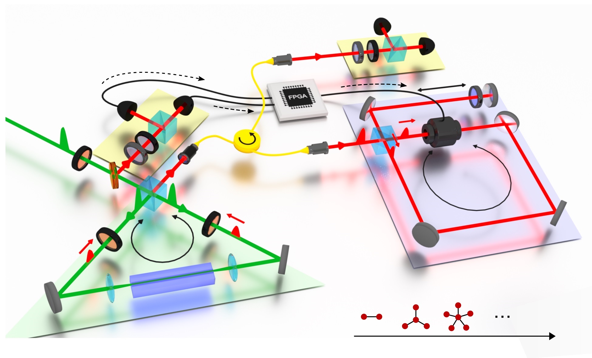
The process of creating photonic qubits begins with generating high-quality single photons or pairs of entangled photons. A qubit can then be defined in several different ways, most often in the photon’s polarization (the orientation of the optical wave) or in the path that the photons travel. Moody and his team can create PICs that control these aspects of the photons, which become the carriers of quantum information and can be manipulated to perform logic operations.
The approach has several advantages over other methods of creating qubits. For instance, the aforementioned environmental effects that can cause qubits to lose their coherence do not affect coherence in photons, which, Moody says, “can maintain that entanglement for a very long time. The challenge is not coherence but, rather, getting the photons to become entangled in the first place.”
“That,” Moody notes, “is because photons don’t naturally interact; rather, they pass right through each other and go their separate ways. But they have to interact in some way to create an entangled state. We’re working on how to create PIC-based quantum light sources that produce high-quality photons as efficiently as possible and then how to get all the photons to interact in a way that allows us to build a scalable quantum processor or new devices for long-distance quantum communications.”
Quantum computers are super efficient, and the photonics approach to quantum technologies is even more so. When Google “demonstrated quantum supremacy” in fall 2019 using the quantum computer built in its Goleta laboratory under the leadership of UCSB physics professor John Martinis, the company claimed that its machine, named Sycamore, could do a series of test calculations in 200 seconds that a super-computer would need closer to 10,000 years to complete. Recently, a Chinese team using a laboratory-scale table-top experiment claimed that, with a photon-based quantum processor, “You could do in two hundred seconds what would take a super-computer 2.5 billion years to accomplish,” Moody said.
Another advantage is that photonics is naturally scalable to thousands and, eventually, millions of components, which can be done by leveraging the wafer-scale fabrication technologies developed for classical photonics. Today, the most advanced PICs comprise nearly five thousand components and could be expanded by a factor of two or four with existing fabrication technologies, a stage of development comparable to that of digital electronics in the 1960s and 1970s. “Even a few hundred components are enough to perform important quantum computing operations with light, at least on a small scale between a few qubits,” said Moody. With further development, quantum photonic chips can be scaled to tens or hundreds of qubits using the existing photonics infrastructure.
Moody’s team is developing a new materials platform, based on gallium arsenide and silicon dioxide, to generate single and entangled photons, and it promises to be much more efficient than comparable systems. In fact, they have a forthcoming paper showing that their new quantum light source is nearly a thousand times more efficient than any other on-chip light source.
In terms of the process, Moody says, “At the macro level, we work on making better light sources and integrating many of them onto a chip. Then, we combine these with on-chip programmable processors, analogous to electronic transistors used for classical logic operations, and with arrays of single-photon detectors to try to implement quantum logic operations with photons as efficiently as possible.”
For more accessible applications, like communications, no computing need occur. “It involves taking a great light source and manipulating a property of the photon states (such as polarization), then sending those off to some other chip that’s up in a satellite or in some other part of the world, which can measure the photons and send a signal back that you can collect,” Moody said.
One catch, for now, is that the single-photon detectors, which are used to signal whether the logic operations were performed, work with very high efficiency when they are on the chip; however, some of them work only if the chip is cooled to cryogenic temperatures.
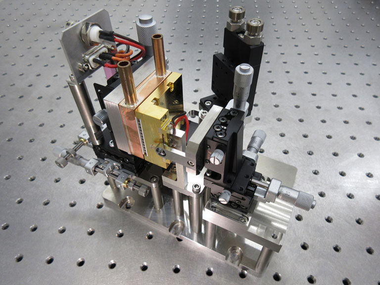
“If we want to integrate everything on chip and put detectors on chip as well, then we’re going to need to cool the whole thing down,” Moody said. “We’re going to build a setup to be able to do that and test the various quantum photonic components designed and fabricated for this. The DURIP award enables exactly this: developing the instrumentation to be able to test large-scale quantum photonic chips from cryogenic temperatures all the way up to room temperature.”
There are also challenges associated with cooling the chip to cryogenic temperatures. Said Moody, “It’s getting this whole platform up and running, interfacing the instrumentation, and making all the custom parts we need to be able to look at large-scale photonic chips for quantum applications at cryogenic temperatures.”


