13 April 2020
Leading research groups in the field of nanophotonics are working toward developing optical transistors – key components for future optical computers. These devices will process information with photons instead of electrons, thus reducing the heat and increasing the operation speed. However, photons do not interact with each other well, which creates a big problem for microelectronics engineers. A group of researchers from ITMO University, together with colleagues, have come up with a new solution to this problem by creating a planar system where photons couple to other particles, which enables them to interact with each other. The principle demonstrated in their experiment can provide a platform for developing future optical transistors. The results of their work are published in Light: Science & Applications.
It is widely known that transistors, key elements of the modern digital world, function thanks to the controlled motion of electrons. Electric currents are used to process, code and transmit information in PCs, smartphones, TVs, and many other devices. This method has been used for decades, but it has several drawbacks. First, electronic devices tend to heat up when they perform a task, which means that part of the energy is wasted as heat and not used for actual work.To fight this heating, we need to equip our devices with coolers, thus wasting even more energy. Second, electronic devices have a limited processing speed.
Some of these issues can be solved by using photons, light particles, instead of electrons. Devices that use photons for information encoding would produce less heat, require less energy, and work faster. That is exactly why scientists all over the world conduct research in the field of optical computers. However, making an optical transistor is not an easy task, because one can not simply replace the electrons in transistors with photons.
“The problem is that photons, unlike electrons, do not interact with each other, so one photon does not control another,” explains Vasily Kravtsov, a leading research fellow at ITMO University. “That is why it is extremely difficult to design a transistor based only on photons.”
Two particles for the price of one
Researchers from over the world suggest different methods to “train” photons to interact with each other. The idea of one of these methods is to couple photons with other particles. A group of researchers from ITMO’s Faculty of Physics and Engineering have demonstrated a new efficient implementation, where photons couple to excitons in single-layer semiconductors. The study was conducted within the framework of a megagrant in collaboration with the University of Sheffield.
“Excitons are elementary excitations in matter,” continues Vasily Kravtsov, a co-author of the paper. “They are formed when an electron is excited, leaving behind an empty valence bond, or an , which, like the nucleus of an atom, is positively charged. Electrons and holes can interact creating a kind of an atom – an exciton. Excitons have dipole moments; to put it simply, they have a negative and a positive pole, which allows them to interact with other excitons. If we couple them to photons strongly enough, we will get polaritons. Polaritons are partly light, meaning that they can be used to transfer information very fast; but at the same time they can interact with each other very well.”
It seems like polaritons are a straightforward solution, and now all we need to do is to create a polariton-based transistor.
However, it is not that easy: we need to design a system where these particles could exist long enough while still maintaining their high interaction strength.
Light traps
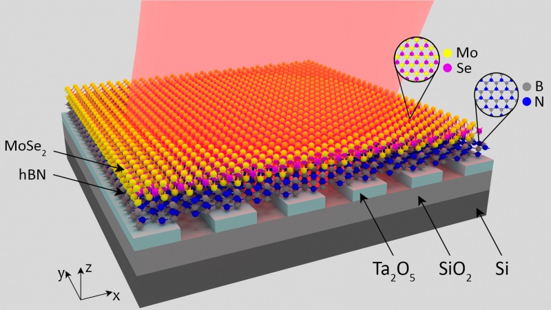
In the labs of ITMO’s Faculty of Physics and Engineering, polaritons are created with the help of a laser, a waveguide, and an extremely thin molybdenum diselenide semiconductor layer.
A three-atom-thick semiconductor layer is placed on a nanophotonic waveguide, with a precise net of very fine grooves engraved on its surface. After that, it is lit up with a red laser to create excitons in the semiconductor. These excitons couple with light particles creating polaritons. The latter are thus temporarily locked in the net of grooves in the waveguide.
“The waveguide is structured in a special way so as to create, loosely speaking, a light trap,” expounds Fedor Benimetskiy, another co-author of the paper. “Picture a set of two mirrors facing each other. Under certain conditions, the light of a specific wavelength will be trapped between them. In our case, the waveguide acts like these two mirrors. When light passes through the semiconductor, it creates polaritons, which are simultaneously light particles and excitons. Thanks to the waveguide’s geometry, these hybrid particles can “live” relatively long.”
Polaritons created in this way do not only exist for relatively long periods of time, but also have extra high nonlinearity, meaning that they actively interact with each other.
“We were able to demonstrate the highly nonlinear behavior of these particles,” continues Vasily Kravtsov. “In other words, polaritons interact with polaritons, they can scatter off each other. We have measured the highest nonlinearity for such systems. It brings us closer to creating an optical transistor, as we now have a planar platform less than 100 nanometers thick, which could be integrated on a chip. As the nonlinearity is rather high, we would not need a powerful laser – a small red light source will suffice, which could also be integrated onto the chip.”
At the moment, however, it is too soon to talk about designing a chip – new research efforts are on the way. The scientists now have to demonstrate that their system can operate at a room temperature, as the experiments so far have been done at -120 C. Moreover, it is important to further extend the lifetime of polaritons in the system.

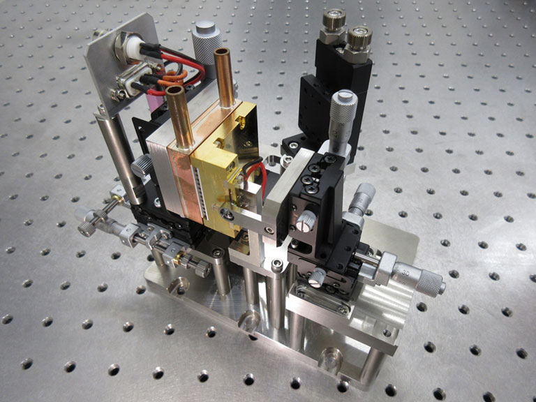
A lab at ITMO’s Faculty of Physics and Engineering
Reference: Vasily Kravtsov, Ekaterina Khestanova, Fedor A. Benimetskiy, Tatiana Ivanova, Anton K. Samusev, Ivan S. Sinev, Dmitry Pidgayko, Alexey M. Mozharov, Ivan S. Mukhin, Maksim S. Lozhkin, Yuri V. Kapitonov, Andrey S. Brichkin, Vladimir D. Kulakovskii, Ivan A. Shelykh, Alexander I. Tartakovskii, Paul M. Walker, Maurice S. Skolnick, Dmitry N. Krizhanovskii & Ivan V. Iorsh, «Nonlinear polaritons in a monolayer semiconductor coupled to optical bound states in the continuum», Light: Science & Applications volume 9, 2020

