Mar 25, 2020
Under DARPA’s Photonics in the Package for Extreme Scalability (PIPES) program, researchers from Intel and Ayar Labs have demonstrated early progress towards improving chip connectivity with photons – or light. Signaling over optical fibers enables the internet today and optical transceivers are ubiquitous in data centers, yet digital systems still rely upon the movement of electrons over metal wires to push data between integrated circuits (ICs) on a board. Increasingly, the limitations of electrical signaling from the chip package restrict overall bandwidth and signaling efficiency, throttling the performance of advanced systems. The PIPES program is exploring ways to expand the use of optical components to address these constraints and enable digital microelectronics with new levels of performance.
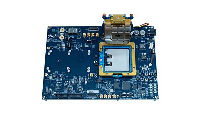
Researchers from Intel and Ayar Labs working on PIPES have successfully replaced the traditional electrical input/output (I/O) of a state-of-the-art field programmable gate array (FPGA) with efficient optical signaling interfaces. The demonstration leverages an optical interface developed by Ayar Labs called TeraPHY, an optical I/O chiplet that replaces electrical serializer/deserializer (SERDES) chiplets. These SERDES chiplets traditionally compensate for limited I/O when there is a need for fast data movement, enabling high-speed communications and other capabilities. Using Intel’s advanced packaging and interconnect technology, the team integrated TeraPHY and the Intel FPGA core within a single package, creating a multi-chip module (MCM) with in-package optics. The integrated solution substantially improves interconnect reach, efficiency, and latency – enabling high-speed data links with single mode optical fibers coming directly from the FPGA. Built in GlobalFoundries’ advanced photonics process, the co-packaged TeraPHY chiplet used for this demonstration is capable of 2 Terabits per second (Tbps) of I/O bandwidth at a small fraction of power compared to electrical I/O.
“This early PIPES program demonstration is a big step towards enabling powerful systems that leverage the advantages of optical signaling,” said Dr. Gordon Keeler, the DARPA program manager leading PIPES. “A key goal of the program is to develop advanced ICs with photonic interfaces capable of driving >100 terabits per second (Tbps) I/O per package at energies below one picojoule per bit (pJ/bit). FPGAs with photonic interfaces will have broad impact, improving high-performance computing, artificial intelligence, large-scale emulation, and DoD-specific capabilities such as advanced radars. With this demonstration, the Intel team has made a solid step towards our goal.”
To accomplish the demonstration, Intel and Ayar Labs’ researchers leveraged technical advances achieved under two other DARPA programs – the Photonically Optimized Embedded Microprocessors (POEM) and Common Heterogeneous Integration and IP Reuse Strategies (CHIPS) programs. Now concluded, the DARPA POEM program sought to develop photonic technologies that could be integrated within embedded microprocessors to enable seamless, energy-efficient, high-capacity communications within and between the microprocessor and dynamic random access memory (DRAM). Ayar Labs’ work under POEM helped generate the first TeraPHY optical I/O chiplet.
Researchers also leveraged low-power signaling standards and chiplet packaging processes developed by Intel under the DARPA CHIPS program. To help address skyrocketing design costs and increase system flexibility, CHIPS is working to develop an ecosystem of discrete modular, reusable IP block that can be assembled into systems using various integration technologies. Critical to this effort was the establishment of a common interface standard, which Intel supplied via the Advanced Interface Bus (AIB). AIB is a publicly available, open interface standard that enables Intel and other silicon IP providers working under the program to easily build chiplets that can inter-operate with each other. The PIPES team used the AIB interface standards to integrate the MCM and in-package optics.
As PIPES progresses, the Intel team will continue to advance performance of the integrated technologies. Through the next phases of the program, all PIPES researchers will focus on enabling aggregate signaling rates to 100 Tbps and beyond, maturing various photonics technologies, and meeting demanding metrics for efficiency, latency, and bandwidth density.

