2020.08.25
The National Institute for Materials Science (NIMS) has developed a memory device capable of storing multiple values using both optical and voltage input values. This technology may be used to significantly increase the capacity of memory devices and applied to the development of various optoelectronic devices. This device composed of layered two-dimensional materials is able to optically control the amount of charge stored in these layers. This technology may be used to significantly increase the capacity of memory devices and applied to the development of various optoelectronic devices.
Memory devices used to store information (e.g., flash memory) play an indispensable role in today’s information society. The recording density of these devices has substantially increased in the past 20 years. In anticipation of widespread adoption of IoT technologies in the near future, it is desirable to accelerate the development of higher speed, larger capacity memory devices. However, the current approach to increasing memory capacity and energy efficiency through silicon microfabrication is about to reach its limits. Development of memory devices with different working principles therefore has been awaited.
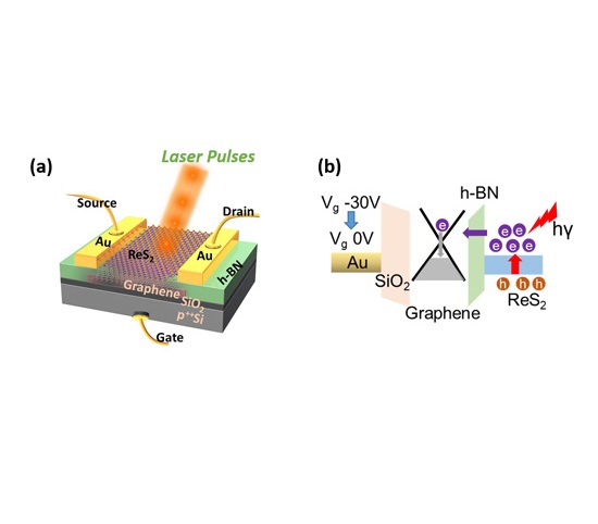
To meet expected technology needs, this research group has developed a transistor memory device composed of layered two-dimensional materials, including rhenium disulfide (ReS2)—a semiconductor—serving as a channel transistor, hexagonal boron nitride (h-BN) used as an insulating tunnel layer and graphene functioning as a floating gate. This device records data by storing charge carriers in the floating gate in a manner similar to conventional flash memory. Hole-electron pairs in the ReS2 layer are prone to excitation when irradiated with light. The number of these pairs can be regulated by changing the intensity of the light. The group succeeded in creating a mechanism that allows the amount of charge in the graphene layer to gradually decrease as the exited electrons once again couple with the holes in this layer. This success enabled the device to operate as a multivalued memory capable of efficiently controlling the amount of stored charge in stages through the combined use of light and voltage. Moreover, this device can operate energy efficiently by minimizing electric current leakage—an achievement made possible by layering two-dimensional materials, thereby smoothening the interfaces between them at an atomic level.
This technology may be used to significantly increase the capacity and energy efficiency of memory devices. It also may be applied to the development of various optoelectronic devices, including optical logic circuits and highly sensitive photosensors capable of controlling the amount of charge stored in them through combined use of light and voltage.
This project was carried out by a research group consisting of Yutaka Wakayama (Leader of the Quantum Device Engineering Group (QDEG), International Center for Materials Nanoarchitectonics (MANA), NIMS), Bablu Mukherjee (Postdoctoral Researcher, QDEG, MANA, NIMS) and Shu Nakaharai (Principal Researcher, QDEG, MANA, NIMS).
This study was conducted in conjunction with another project entitled “Development of a ultra-sensitive photosensor using two-dimensional atomic film layers” funded by the Grant-in-Aid for JSPS Fellows.
This research was published in the online version of Advanced Functional Materials at 12:00 pm on August 25, 2020, Central European Time (7:00 pm on August 25, Japan Time).
(”Laser-assisted multilevel non-volatile memory device based on 2D van-der-Waals fewlayer-ReS2/h-BN/Graphene Heterostructures” Bablu Mukherjee, Amir Zulkefli, Kenji Watanabe, Takashi Taniguchi, Yutaka Wakayama, Shu Nakaharai; Journal: Advanced Functional Materials [August 25, 2020]; DOI : 10.1002/adfm.202001688)

