03/02/2020
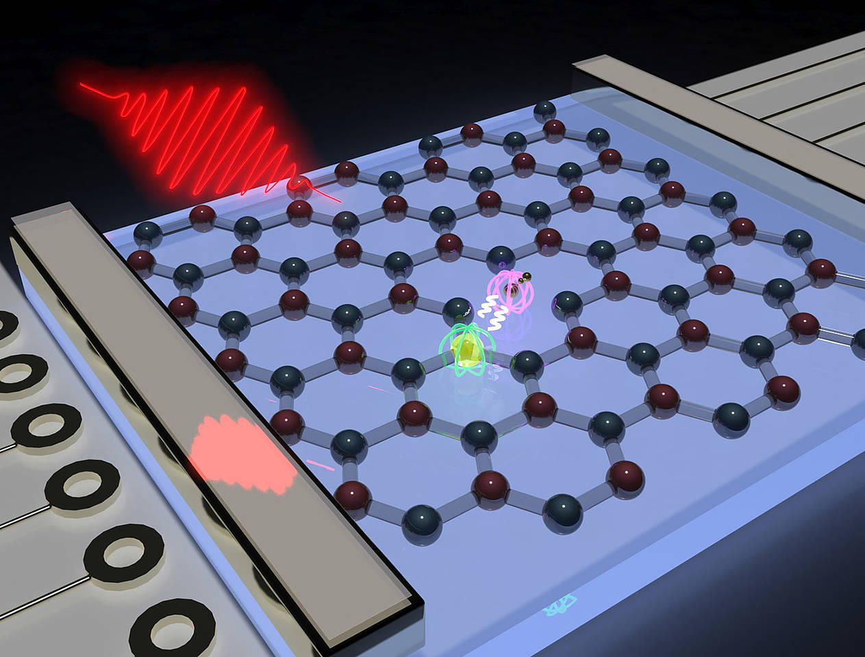
Although boron nitride looks very similar to graphene in structure, it has completely different optoelectronic properties. Its constituents, the elements boron and nitrogen, arrange – like carbon atoms in graphene – a honeycomb-like hexagonal structure. They arrange themselves in two-dimensional layers that are only one atomic layer thick. The individual layers are only weakly coupled to each other by so-called van der Waals forces and can therefore be easily separated from each other.
Publication in Nature Materials
Physicists from Julius-Maximilians-Universität Würzburg (JMU) in Bavaria, Germany, in cooperation with the Technical University of Sydney in Australia have now succeeded for the first time in experimentally demonstrating so-called spin centers in a boron nitride crystal. Professor Vladimir Dyakonov, holder of the Chair of Experimental Physics VI at the Institute of Physics, and his team were responsible for this on the JMU side and carried out the crucial experiments. The results of the work have been published in the renowned scientific journal Nature Materials.
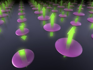
In the layered crystal lattice of boron nitride the physicists found a special defect – a missing boron atom – which exhibits a magnetic dipole moment, also known as a spin. Furthermore, it can also absorb and emit light and is therefore also called color center. To study the magneto-optical properties of the quantum emitter in detail, JMU scientists have developed a special experimental technique that uses the combination of a static and a high-frequency magnetic field.
A little luck is needed
"If you vary the frequency of the alternating magnetic field, at some point you hit exactly the frequency of the spin, and the photoluminescence changes dramatically," explains Dyakonov. A bit of luck is necessary, however, since it is difficuilt to predict at which frequencies one has to search for unknown spin states. Dyakonov and his team had discovered these centers in the 2D crystalline system, which had previously only been predicted theoretically. Among other things, they were able to demonstrate spin polarization, i.e. the alignment of the magnetic moment of the defect under optical excitation – even at room temperature.
This makes the experiments interesting for technical applications as well: Scientists around the world are currently working on finding a solid-state system in which the spin state can be aligned, manipulated on demand and later read-out optically or electrically. "The spin center we have identified in boron nitride meets these requirements," adds Dyakonov. Because it has a spin and additionally absorbs and emits light, it is a quantum bit that can be used in quantum sensing and quantum information. New navigation technology could also work with this technology, which is why space agencies such as DLR and NASA are conducting intensive research on this topic, too.
Material design by the Lego brick principle
For the basic scientist, the 2D materials are also exciting from another point of view. They have very special layer structure, combined with the only weak bonding of the layers to each other, offers the possibility of constructing different stacking sequences from different semiconductors. "If you then place a defect in one of these layers, we call it a spin probe, this can help to understand the properties of the adjacent layers, but also to change the physical properties of the entire stack," says Dyakonov.
In a next step, Dyakonov and his colleagues therefore want to produce, among other things, heterostructures made of multilayer semiconductors with a boron nitride layer as an intermediate layer. They are convinced: "If the atomically thin layers of boron nitride, which are 'decorated' with individual spin centers, can be produced and incorporated into a heterostructure, it will be possible to design artificial two-dimensional crystals based on Lego brick principles and investigate their properties.”
Funding
This work was funded by several funding agencies, including the German Research Foundation (DFG) and the Alexander von Humboldt Foundation. It is closely related to the Cluster of Excellence ct.qmat (Würzburg-Dresden), in which Vladimir Dyakonov is a Principle Investigator.
Publication
Initialization and read-out of intrinsic spin defects in a von der Waals crystal at room temperature. Andreas Gottschol et al, Nature Materials, DOI: 10.1038/s41563-020-0619-6 https://www.nature.com/articles/s41563-020-0619-6
By Gunnar Bartsch

