08.04.2020
For the past 50 years, researchers around the globe have been looking for a way to make lasers with silicon or germanium. A team from the Technical University of Eindhoven (TU/e) and the Technical University of Munich (TUM) has now succeeded in developing light-emitting, silicon-germanium alloys. As a result, the development of a silicon laser capable of integration into today's chips is within reach for the first time.
Electronic chips produce heat when processing data. The laptop starts to feel uncomfortably hot on the user's knees; data centers need energy-hungry cooling equipment. The solution may lie in the field of photonics – because light pulses do not emit heat.
For the past half century, this insight has driven efforts by researchers to build silicon or germanium-based lasers – so far in vain. Silicon, the workhorse of the chip industry, normally crystallizes in a cubic crystal lattice. In this form it is not suitable for converting electrons into light.
Together with colleagues from the Technical University of Munich and the universities in Jena and Linz, researchers at the Technical University of Eindhoven have now developed alloys made of germanium and silicon capable of emitting light.
The crucial step was the ability to produce germanium and alloys from germanium and silicon with a hexagonal crystal lattice. “This material has a direct band gap, and can therefore emit light itself,” says Prof. Jonathan Finley, Professor of Semiconductor Quantum Nanosystems at TUM.
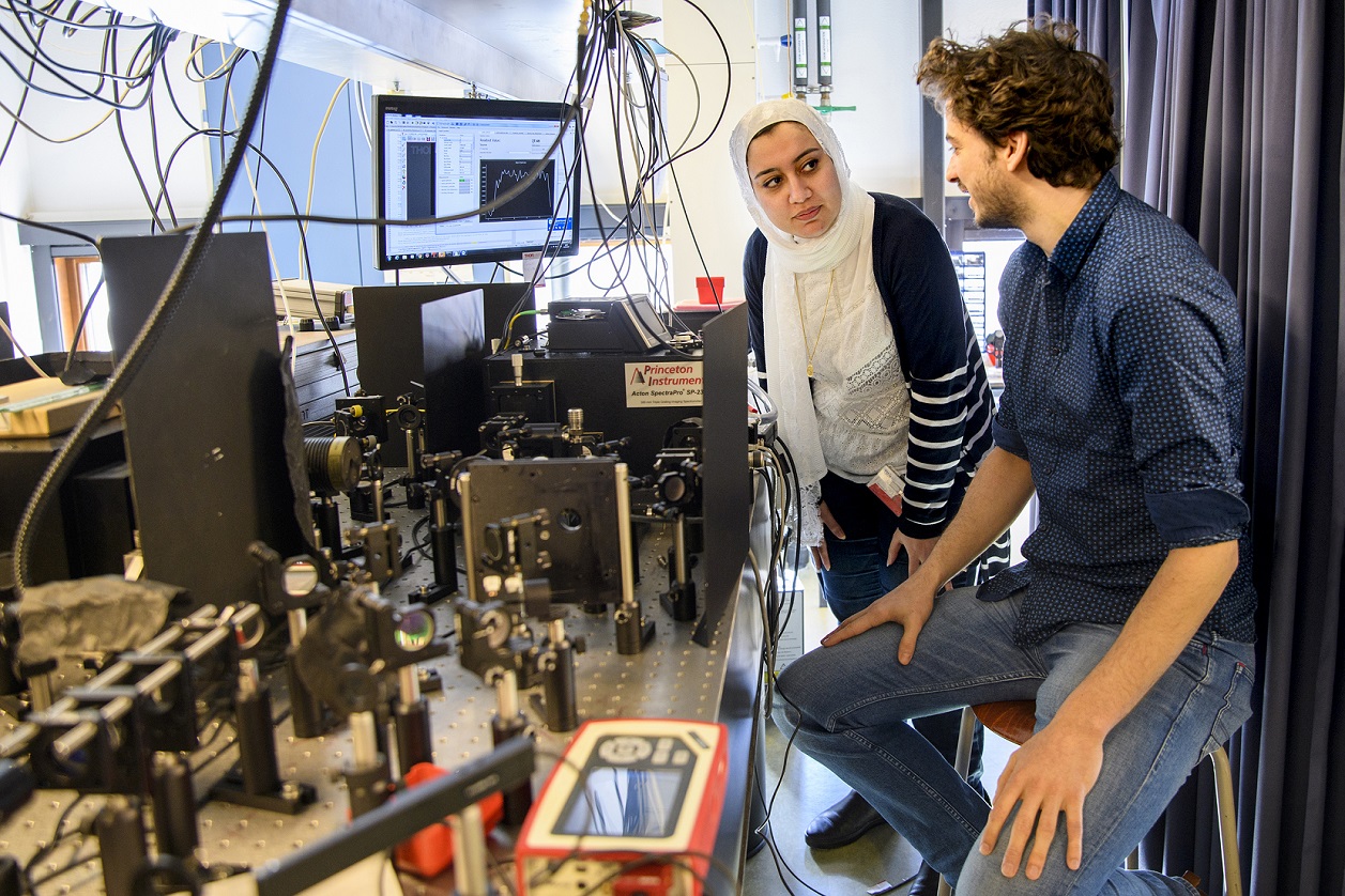
First authors Elham Fadaly (left) and Alain Dijkstra (right) at their optical setup to measure the emission of light from the hexagonal-SiGe nanowires.
Sicco van Grieken, SURF / TU/e
The template trick
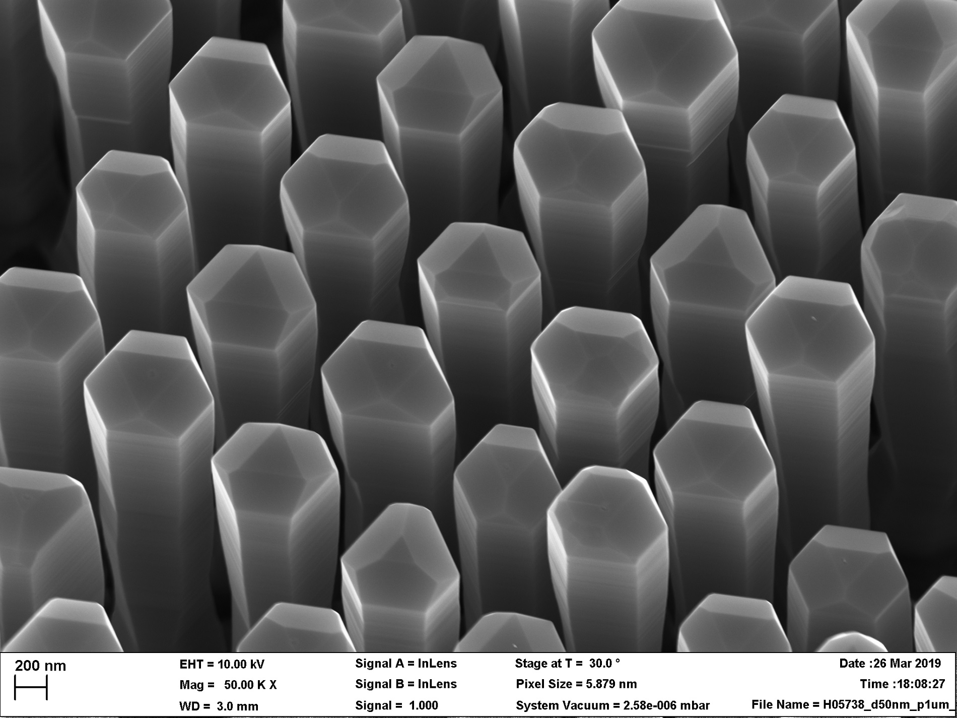
Prof. Erik Bakkers and his team at TU Eindhoven first produced hexagonal silicon back in 2015. They started by growing a hexagonal crystal structure with nanowires made of another material. This served as a template for a germanium-silicon shell on which the underlying material imposed its hexagonal crystal structure.
Initially, however, these structures could not be stimulated to emit light. Through the exchange of ideas with colleagues at the Walter Schottky Institute at the Technical University of Munich, who analyzed the optical characteristics with each successive generation, the production process was finally optimized to a grade of perfection where the nanowires were indeed capable of emitting light.
“In the meantime, we have achieved properties almost comparable to indium phosphide or gallium arsenide,” says Prof. Bakkers. As a result, it appears to be just a matter of time before a laser made from germanium-silicon alloys and capable of integration into conventional production processes is developed.
“If we can implement on-chip and inter-chip electronic communications by optical means, speeds can be increased by a factor of up to 1,000,” says Jonathan Finley. “In addition, the direct combination of optics and electronics could drastically reduce the cost of chips for laser-based radar in self-driving cars, chemical sensors for medical diagnostics, and air and food quality measurements.”
Publication:
Direct Bandgap Emission from Hexagonal Ge and SiGe Alloys
E. M. T. Fadaly, A. Dijkstra, J. R. Suckert, D. Ziss, M. A. J. v. Tilburg, C. Mao, Y. Ren, V. T. v. Lange, S. Kölling, M. A. Verheijen, D. Busse, C. Rödl, J. Furthmüller, F. Bechstedt, J. Stangl, J. J. Finley, S. Botti, J. E. M. Haverkort, E. P. A. M. Bakkers.
Nature, 8. April 2020 – DOI: 10.1038/s41586-020-2150-y
Link: https://www.nature.com/articles/s41586-020-2150-y
Further information:
The research project received funding from the European Union (EU) project, SiLAS, the Marie Sklodowska Curie Programme of the EU, the Dutch Research Council (NWO), the Solliance Initiative of the Energy research Centre of the Netherlands (ECN), the Holst Center, the TU/e, the Netherlands Organization for Applied Scientific Research (TNO), the Interuniversity Microelectronics Centre (IMEC), the Forschungszentrum Jülich and the province of North Brabant in the Netherlands. The Deutsches Elektronen Synchrotron (DESY) in Hamburg provided measurement time on the PETRA III facility. Theoretical calculations were carried out on the SuperMUC high-performance computer at the Leibniz Supercomputing Center in Garching, Germany.

