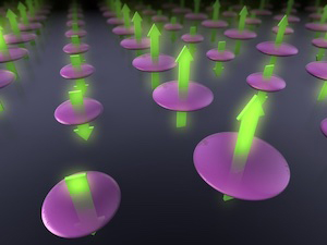
(Hoboken, N.J. – Monday, Oct. 29, 2018) -- Household lightbulbs give off a chaotic torrent of energy, as trillions of miniscule light particles – called photons – reflect and scatter in all directions. Quantum light sources, on the other hand, are like light guns that fire single photons one by one, each time they are triggered, enabling them to carry hack-proof digital information - technology attractive to industries such as finance and defense.
Now, researchers at Stevens Institute of Technology and Columbia University have developed a scalable method for creating large numbers of these quantum light sources on a chip with unprecedented precision that not only could pave the way for the development of unbreakable cryptographic systems but also quantum computers that can perform complex calculations in seconds that would take normal computers years to finish.
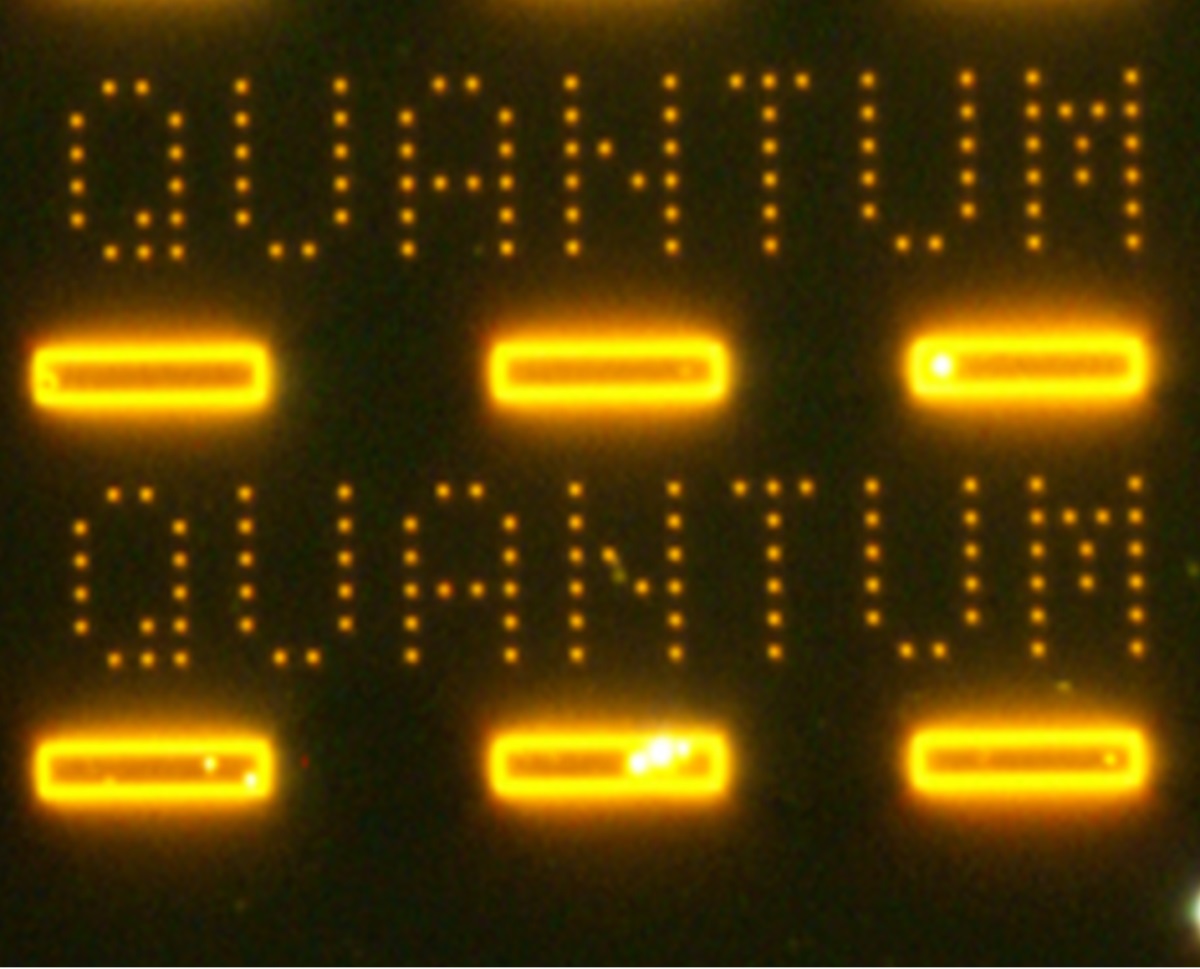 A chip that shows the word quantum. Each dot represents a single quantum light source, demonstrating the scalability and precision of the technique.
“The search for scalable quantum light sources has been going on for 20 years, and more recently has become a national priority,” says Stefan Strauf, who led the work and is also director of Stevens’ Nanophotonic Lab. “This is the first time anyone has achieved a level of spatial control combined with high efficiency on a chip that is scalable, all of which are needed to realize quantum technologies."
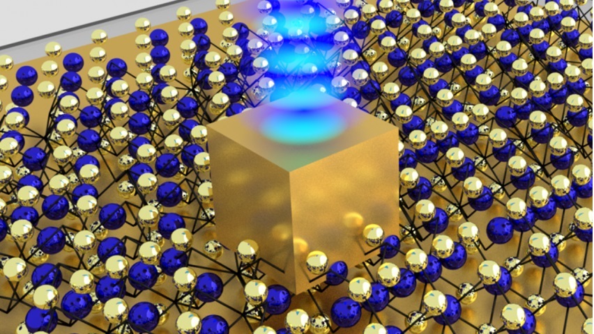
The work, to be reported in the Oct. 29 advance online issue of Nature Nanotechnology, describes a new method for creating quantum light sources on demand in any desired location on a chip, by stretching an atom-thin film of semiconducting material over nanocubes made of gold. Like taut cling-wrap, the film stretches over the corners of the nanocubes, imprinting defined locations where single-photon emitters form.
Past research has tested methods for producing quantum emitters in defined locations, but these designs were not scalable or efficient at triggering single photons frequently enough to be practically useful. Strauf and his team changed all that by becoming the first to combine spatial control and scalability with the ability to efficiently emit photons on demand.
To achieve these capabilities, Strauf’s team designed a unique approach where the gold nanocube serves a dual purpose: it imprints the quantum emitter on the chip and it acts as an antenna around it. By creating the quantum emitters in between the gold nanocube and mirror, Strauf left a five-nanometer narrow gap – 20,000 times smaller than the width of a sheet of paper.
“This tiny space between the mirror and nanocube creates an optical antenna that funnels all the photons into that five-nanometer gap, thereby concentrating all the energy” says Strauf. “Essentially, it provides the necessary boost for the single photons to be emitted rapidly from the defined location and in the desired direction.”
To further improve the efficiency of the quantum light sources, Strauf teamed up with Katayun Barmak and James Hone, of Columbia University, who developed a technique for growing semiconductor crystals that are nearly free of defects. Using these unique crystals, Stevens’ graduate student Yue Luo built rows of quantum emitters on a chip by stretching the atom-thin material over the nanocubes. The nanoantennas are formed by attaching the mirror, on the bottom side of the nanocube.
The result: a record-high firing of 42 million single photons per second; in other words, every second trigger created a photon on demand, compared to only one in 100 triggers previously.
Though tiny, the emitters are remarkably tough. “They’re astonishingly stable,” Strauf says. “We can cool them and warm them and disassemble the resonator and reassemble it, and they still work.” Most quantum emitters must be kept chilled to -273°C but the new technology works up to -70°C. “We’re not yet at room temperature,” says Strauf, “but current experiments show that it’s feasible to get there.”
-- Stevens --
About Stevens Institute of Technology
Stevens Institute of Technology is a premier, private research university situated in Hoboken, New Jersey overlooking the Manhattan skyline. Since our founding in 1870, technological innovation has always been the hallmark and legacy of Stevens’ education and research. Within the university’s three schools and one college, 6,900 undergraduate and graduate students collaborate closely with faculty in an interdisciplinary, student-centric, entrepreneurial environment. Academic and research programs spanning business, computing, engineering, the arts and other fields actively advance the frontiers of science and leverage technology to confront our most pressing global challenges. The university is consistently ranked among the nation’s elite for return on tuition investment, career services and the mid-career salaries of alumni.

