15.01.2018
By: Felix Würsten
ETH physicists have developed a silicon wafer that behaves like a topological insulator when stimulated using ultrasound. They have thereby succeeded in turning an abstract theoretical concept into a macroscopic product.
The usual procedure goes like this: you have a complex physical system and attempt to explain its behaviour through as simple a model as possible. Sebastian Huber, Assistant Professor at the Institute for Theoretical Physics, has shown that this procedure also works in reverse: he develops macroscopic systems that exhibit exactly the same properties predicted by theory, but which have not yet been observed at this level.
He succeeded in creating an illustrative example two and a half years ago. Together with his team, he built a mechanical device made of 270 pendulums connected by springs in such a way that the installation behaves like a topological insulator. This means that the pendulum and springs are positioned so that a vibrational excitation from the outside only moves the pendulums at the edges of the installation, but not the ones in the middle (as ETH News reported).
Vibration only in the corners
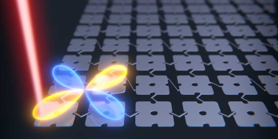
The new project, which will be published this week in the journal Nature], is also focused on a macroscopic system. This time, however, he created no large mechanical device, but a much more manageably-sized object. With his team, Huber created a 10 x 10 centimetre silicon wafer that consists of 100 small plates connected to each other via thin beams. The key aspect is that when the wafer is stimulated using ultrasound, only the plates in the corners vibrate; the other plates remain still, despite their connections.
Huber drew his inspiration for the new material from a work published around a year ago by groups from Urbana-Champaign and Princeton; the researchers presented a new theoretical approach for a second-order topological insulator. “In a conventional topological insulator, the vibrations only spread across the surface, but not inside,” explains Huber. “The phenomenon is reduced by one dimension.” In the case of the pendulum installation, this means that the two-dimensional arrangement led to a one-dimensional vibration pattern along the edges.
In a second-order topological insulator, however, the phenomenon is reduced by two dimensions. Accordingly, with a two-dimensional silicon wafer, the vibration no longer occurs along the edges, but only in the corners, at a zero-dimensional point. “We are the first to succeed in experimentally creating the predicted higher-order topological insulator,” says Huber.
A new theoretical concept
Huber has again created something that behaves in exactly the way predicted by the theory. To solve this “inverse problem”, he used a systematic process that he developed together with the group led by Chiara Daraio, now a professor at Caltech, and which he has published this week in the journal Nature Materials. Broadly speaking, Huber shows how a theoretically predicted functionality can be turned into concrete geometry. “In our example, we tested it using mechanical vibrations, by coupling elements with clearly defined modes of vibration using weak links,” says Huber. “But the process can also be transferred to other applications, such as to optical or electrical systems.”
Expansion to the third dimension
Huber already has clear plans for how to proceed: he wants to achieve a three-dimensional second-order topological insulator, in which the vibrations can be transmitted one-dimensionally. He recently received a Consolidator Grant from the European Research Council (ERC) for this project. Huber explains the basic idea: “We stack a number of these two-dimensional structures on top of each other, so that a three-dimensional form emerges. In this form, information or energy can be conducted from point A to point B through a one-dimensional channel.”
Huber can think of a few possible applications. For example, such new topological insulators could be used to build robust and precise waveguides for communications networks. They could also be of use in the energy sector, for example for energy harvesting, in which energy from a diffuse surrounding source is focused for technological use.
Also of interest to theoreticians
Huber’s results will not only be of interest to engineers and materials researchers, but also theoretical physicists. “The key finding from a theoretical viewpoint is that certain second-order topological insulators cannot be mathematically described as a dipole, as conventional topological insulators are, but as quadrupoles, which are far more complex,” explains Huber. “The fact that we have been able to implement this experimentally in a macroscopic structure for the first time is therefore also a breakthrough for theoreticians.”
References
Serra-Garcia M, Peri V, Süsstrunk R, Bilal OR, Larsen T, Villanueva LG, Huber SD: Observation of a phononic quadrupole topological insulator. Nature 2018, doi: 10.1038/nature25156
Matlack KH, Serra-Garcia M. Palermo A,Huber SD, Daraio C: Designing perturbative metamaterials from discrete models. Nature Materials 2018, doi: 10.1038/s41563-017-0003-3

