MARCH 19, 2018
By Ben Brumfield
[Yes, HOIP quantum properties look extremely robust, and their physics are mystifying]
Some novel materials that sound too good to be true turn out to be true and good. An emergent class of semiconductors, which could affordably light up our future with nuanced colors emanating from lasers, lamps, and even window glass, could be the latest example.
These materials are very radiant, easy to process from solution, and energy-efficient. The nagging question of whether hybrid organic-inorganic perovskites (HOIPs) could really work just received a very affirmative answer in a new international study led by physical chemists at the Georgia Institute of Technology.
The researchers observed in an HOIP a “richness” of semiconducting physics created by what could be described as electrons dancing on chemical underpinnings that wobble like a funhouse floor in an earthquake. That bucks conventional wisdom because established semiconductors rely upon rigidly stable chemical foundations, that is to say, quieter molecular frameworks, to produce the desired quantum properties.
“We don’t know yet how it works to have these stable quantum properties in this intense molecular motion,” said first author Felix Thouin, a graduate research assistant at Georgia Tech. “It defies physics models we have to try to explain it. It’s like we need some new physics.”
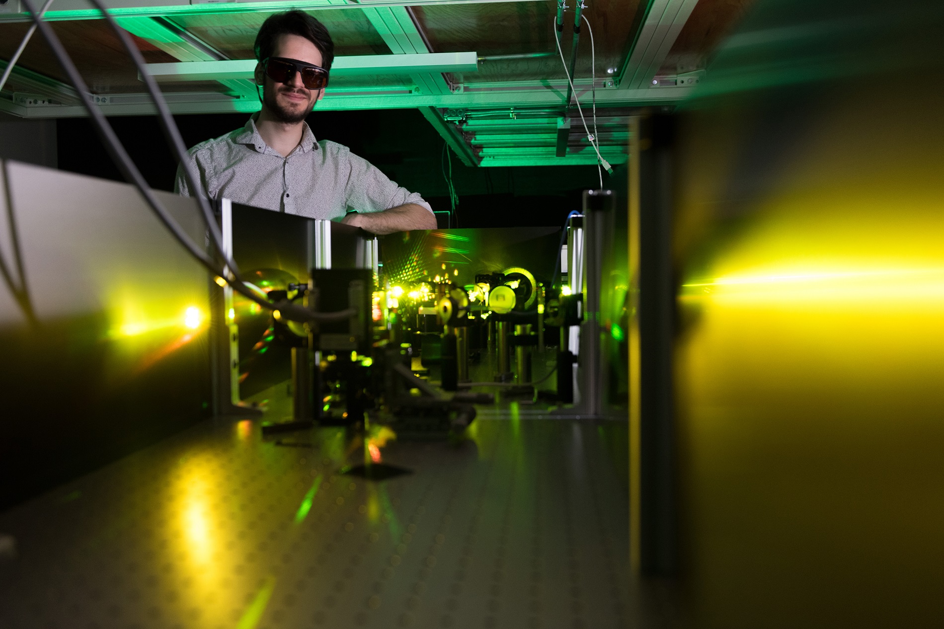
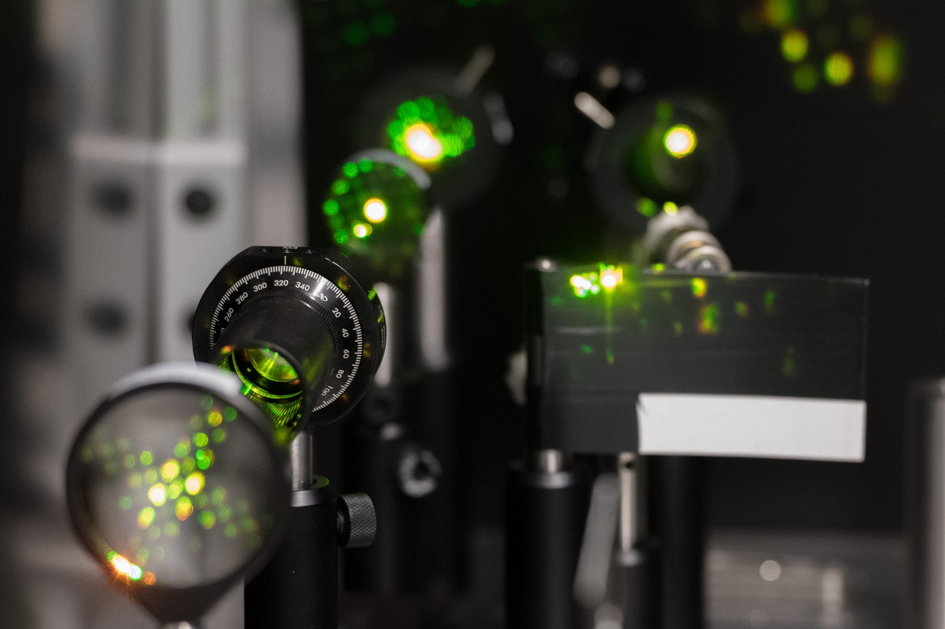
Georgia Tech graduate research assistant Felix Thouin in Carlos Silva's lab stands at a table where laser light in the visible range undergoes processing to ready it for use in measuring materials qualities. Credit: Georgia Tech / Allison Carter
Quantum properties surprise
Their gyrating jumbles have made HOIPs challenging to examine, but the team of researchers from a total of five research institutes in four countries succeeded in measuring a prototypical HOIP and found its quantum properties on par with those of established, molecularly rigid semiconductors, many of which are graphene-based.
“The properties were at least as good as in those materials and may be even better,” said Carlos Silva, a professor in Georgia Tech’s School of Chemistry and Biochemistry. Not all semiconductors also absorb and emit light well, but HOIPs do, making them optoelectronic and thus potentially useful in lasers, LEDs, other lighting applications, and also in photovoltaics.
The lack of molecular-level rigidity in HOIPs also plays into them being more flexibly produced and applied.
Silva co-led the study with physicist Ajay Ram Srimath Kandada. Their team published the results of their study on two-dimensional HOIPs on March 8, 2018, in the journal Physical Review Materials. Their research was funded by EU Horizon 2020, the Natural Sciences and Engineering Research Council of Canada, the Fond Québécois pour la Recherche, the Research Council of Canada, and the National Research Foundation of Singapore.
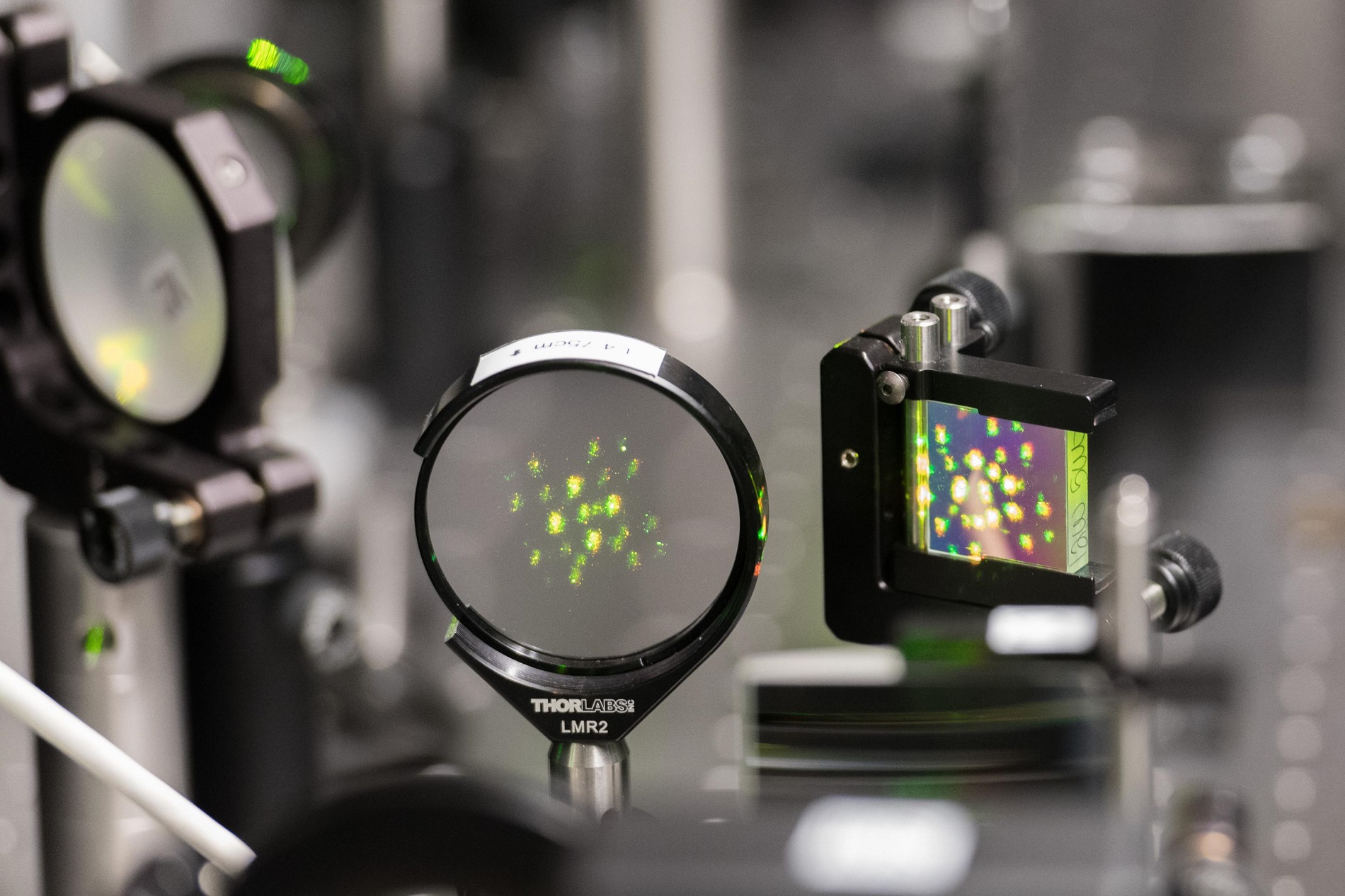
Laser in the visible range to test materials properties
Laser light in the visible range is processed for use in the testing of quantum properties in materials in Carlos Silva's lab at Georgia Tech. Credit: Georgia Tech / Allison Carter
The ‘solution solution’
Commonly, semiconducting properties arise from static crystalline lattices of neatly interconnected atoms. In silicon, for example, which is used in most commercial solar cells, they are interconnected silicon atoms. The same principle applies to graphene-like semiconductors.
“These lattices are structurally not very complex,” Silva said. “They’re only one atom thin, and they have strict two-dimensional properties, so they’re much more rigid.”
“You forcefully limit these systems to two dimensions,” said Srimath Kandada, who is a Marie Curie International Fellow at Georgia Tech and the Italian Institute of Technology. “The atoms are arranged in infinitely expansive, flat sheets, and then these very interesting and desirable optoelectronic properties emerge.”
These proven materials impress. So, why pursue HOIPs, except to explore their baffling physics? Because they may be more practical in important ways.
“One of the compelling advantages is that they’re all made using low-temperature processing from solutions,” Silva said. “It takes much less energy to make them.”
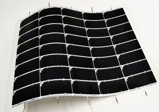
By contrast, graphene-based materials are produced at high temperatures in small amounts that can be tedious to work with. “With this stuff (HOIPs), you can make big batches in solution and coat a whole window with it if you want to,” Silva said.
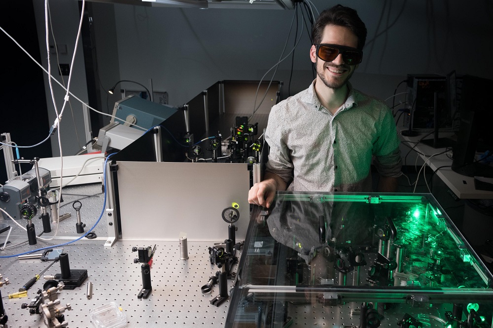
Felix Thouin in Carlos Silva lab
Graduate research assistant Felix Thouin stands at a protective laser casing in the lab of Carlos Silva, in which laser light is adjusted and filtered to desirable qualities in the visible range. Behind Thouin, visible range laser light undergoes more processing to ready it for use in measuring materials qualities. Credit: Georgia Tech / Allison Carter
Funhouse in an earthquake
For all an HOIP’s wobbling, it’s also a very ordered lattice with its own kind of rigidity, though less limiting than in the customary two-dimensional materials.
“It’s not just a single layer,” Srimath Kandada said. “There is a very specific perovskite-like geometry.” Perovskite refers to the shape of an HOIPs crystal lattice, which is a layered scaffolding.
“The lattice self-assembles,” Srimath Kandada said, “and it does so in a three-dimensional stack made of layers of two-dimensional sheets. But HOIPs still preserve those desirable 2D quantum properties.”
Those sheets are held together by interspersed layers of another molecular structure that is a bit like a sheet of rubber bands. That makes the scaffolding wiggle like a funhouse floor.
“At room temperature, the molecules wiggle all over the place. That disrupts the lattice, which is where the electrons live. It’s really intense,” Silva said. “But surprisingly, the quantum properties are still really stable.”
Having quantum properties work at room temperature without requiring ultra-cooling is important for practical use as a semiconductor.
Going back to what HOIP stands for -- hybrid organic-inorganic perovskites – this is how the experimental material fit into the HOIP chemical class: It was a hybrid of inorganic layers of a lead iodide (the rigid part) separated by organic layers (the rubber band-like parts) of phenylethylammonium (chemical formula (PEA)2PbI4).
The lead in this prototypical material could be swapped out for a metal safer for humans to handle before the development of an applicable material.
Electron choreography
HOIPs are great semiconductors because their electrons do an acrobatic square dance.
Usually, electrons live in an orbit around the nucleus of an atom or are shared by atoms in a chemical bond. But HOIP chemical lattices, like all semiconductors, are configured to share electrons more broadly.
Energy levels in a system can free the electrons to run around and participate in things like the flow of electricity and heat. The orbits, which are then empty, are called electron holes, and they want the electrons back.
“The hole is thought of as a positive charge, and of course, the electron has a negative charge,” Silva said. “So, hole and electron attract each other.”
The electrons and holes race around each other like dance partners pairing up to what physicists call an “exciton.” Excitons act and look a lot like particles themselves, though they’re not really particles.
Hopping biexciton light
In semiconductors, millions of excitons are correlated, or choreographed, with each other, which makes for desirable properties, when an energy source like electricity or laser light is applied. Additionally, excitons can pair up to form biexcitons, boosting the semiconductor’s energetic properties.
“In this material, we found that the biexciton binding energies were high,” Silva said. “That’s why we want to put this into lasers because the energy you input ends up to 80 or 90 percent as biexcitons.”
Biexcitons bump up energetically to absorb input energy. Then they contract energetically and pump out light. That would work not only in lasers but also in LEDs or other surfaces using the optoelectronic material.
“You can adjust the chemistry (of HOIPs) to control the width between biexciton states, and that controls the wavelength of the light given off,” Silva said. “And the adjustment can be very fine to give you any wavelength of light.”
That translates into any color of light the heart desires.
Like this article? Get our email newsletter here.
ALSO read this materials article: Turbocharging Fuel Cells with a Multifunctional NanoCatalyst
Coauthors of this paper were Stefanie Neutzner and Annamaria Petrozza from the Italian Institute of Technology (IIT); Daniele Cortecchia from IIT and Nanyang Technological University (NTU), Singapore; Cesare Soci from the Centre for Disruptive Photonic Technologies, Singapore; Teddy Salim and Yeng Ming Lam from NTU; and Vlad Dragomir and Richard Leonelli from the University of Montreal. The research was funded by: The EU Horizon 2020’s Curie Fellowship (project 705874); the EU 2020 Research and Innovation Program (Grant #643238 SYNCHRONICS); the Natural Sciences and Engineering Research Council of Canada and Fond Québécois pour la Recherche: Nature et Technologies; the Canadian Foundation for Innovation, the Natural Science and Engineering Research Council of Canada; and the National Research Foundation of Singapore (NRF-CRP14-2014-03). Any findings and opinions are those of the authors and not necessarily of the funding agencies.

