16.11.2016
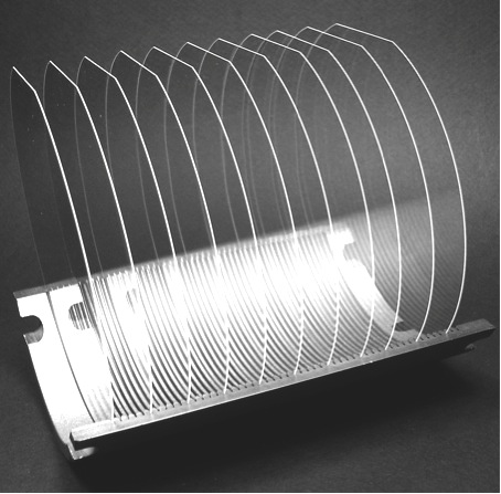
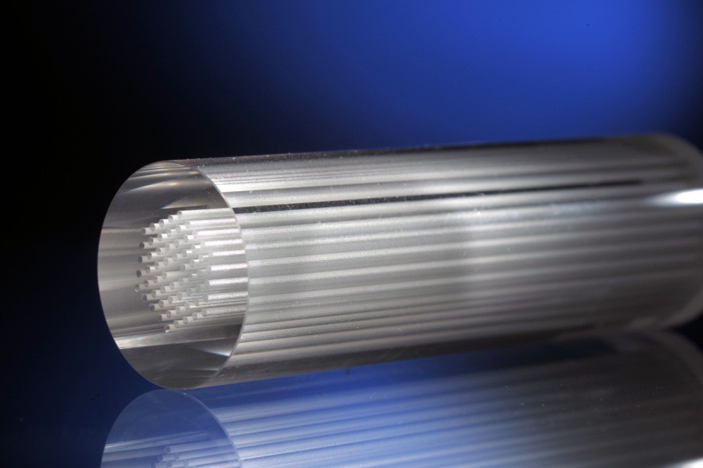
Plan Optik AG the leading manufacturer of glass and quartz wafers now offers fused silica wafers from one of the purest materials: ULTRA HIGH PURITY FUSED SILICA.
Ultra High Purity Fused Silica has an impurity level (trace metal content) of less than 0.2 ppm. This is the lowest impurity level available in the market which makes it suitable for CMOS processes as well as for UV transmitting optics or lithography. The UV transmission at 200 nm is more than 90% (including reflection losses).
In addition to the low impurity level the material got a hydroxyl content (OH) of also less than 0.2 ppm. This extremely low hydroxyl content leads to a very low absorption on infrared light which increases the maximum operating temperature to 1200 degC.
Plan Optik AG produces wafers from this high purity material in 100, 150 and 200 mm diameter. Thickness of these wafers ranges from 0.1 mm to 3 mm. These wafers are double side polished using Plan Optik's sub nanometer roughness polishing process (Ra < 0.5 nm).
Many diameter/thickness combinations are available from stock for immediate supply. Customized wafers or other substrates from this material are available as well.

