29 November 2017
By forcing light to go through a smaller gap than ever before, researchers have paved the way for computers based on light instead of electronics.
Light is desirable for use in computing because it can carry a higher density of information and is much faster and more efficient than conventional electronics. However, light does not easily interact with itself, so while it can be used to move information quickly, it is not very good at processing information.
For example, light is currently used to transfer information over long distances, such as in transatlantic cables and fibre optics, which deliver fast internet. However, once the information reaches your computer, electronics are needed to convert and process it.
In order to use light for processing on microchips, several important obstacles need to be overcome. For example, light can be made to interact using particular materials, but only over relatively long distances. Now, however, a team from Imperial College London has made a significant step forward by reducing the distance over which light can interact by 10,000 fold.
This means that what previously would have taken centimetres to achieve can now be realised on the micrometre (one millionth of a metre) scale, bringing optical processing into the range of electrical transistors, which currently power personal computers. The results are published today in the journal Science.
Dr Michael Nielsen, from the Department of Physics at Imperial, said: “This research has ticked one of the boxes needed for optical computing.
“Because light does not easily interact with itself, information sent using light must be converted into an electronic signal, and then back into light. Our technology allows processing to be achieved purely with light.”
Normally when two light beams cross each other the individual photons do not interact or alter each other, as two electrons do when they meet. Special nonlinear optical materials can make photons interact, but the effect is usually very weak. This means a long span of the material is needed to gradually accumulate the effect and make it useful.
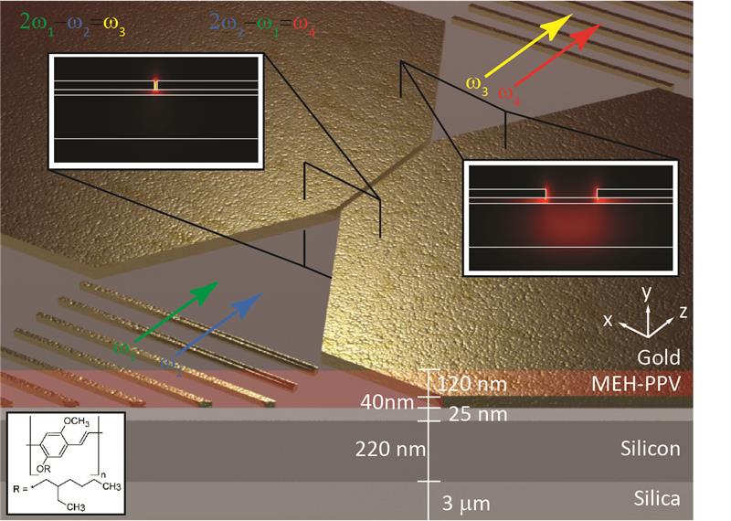
However, by squeezing light into a channel only 25 nanometres (25 billionths of a metre) wide, the Imperial team increased its intensity. This allowed the photons to interact more strongly over a short distance, changing the property of the light that emerged from the other end of the one-micrometre-long channel.
Controlling light on such a small scale is an important step is the construction of computers that use light instead of electronics. Electronic computing is at the limit of efficiency; while it is possible to make a faster electronic processor, the energy cost of moving memory data around the computer any faster is too high.
To make computers more powerful, processors are instead made smaller, so more can fit into the same space, without increasing processing speed. Optical processing can generate little to no heat, meaning using light can make computers much faster and more efficient.
The team achieved the effect by using a metal channel to focus the light inside a polymer previously investigated for use in solar panels. Metals are more efficient at focussing light than traditional transparent materials, and are also used to direct electrical signals.
The new technology is therefore not only more efficient, but can be integrated with current electronics.
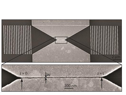
Fabricated structure of W=25 nm and L=2μm with grating couplers and 30° tapers. Images taken by scanning electron microscopy. Nielsen et al., 2017/Imperial College London
Dr Rupert Oulton, from the Department of Physics at Imperial said: “The use of light to transfer information has gotten closer to our homes. It was first used in transatlantic cables, where capacity was most crucial, but now fibre optic broadband is being installed in more and more streets in the UK. As our hunger for more data increases, optics will need to come into the home, and eventually inside our computers.”
As well as providing an important step towards optical computing, the team’s achievement potentially solves a longstanding problem in nonlinear optics. Since interacting light beams with different colours pass through a nonlinear optical material at different speeds, they can become ‘out of step’ and the desired effect can be lost.
In the new device, because the light travels such a short distance, it does not have time to become out of step. This eliminates the problem, and allows nonlinear optical devices to be more versatile in the type of optical processing that can be achieved.
-
Sidebar: What is nonlinear optics?
The process by which photons are made to interact is called nonlinear optics. Technologies that use it are quite common – a simple example is a green laser pointer. It is difficult to make a green laser directly, so nonlinear optical crystals are used to convert infrared light to green.
Invisible infrared light from a semiconductor laser diode, powered by batteries, is passed through a crystal that allows photons to interact with each other. Here, two infrared (invisible) photons join to make a single photon with twice the energy, corresponding to green light.

