07/21/2017
A team of physicists featuring researchers from MIPT and ITMO University has conducted a comparative analysis of a range of materials to determine if they are applicable to dielectric nanophotonics. Their systematic study produced results that can optimize the use of known materials for building optical nanodevices, as well as encourage the search for new materials with superior properties.
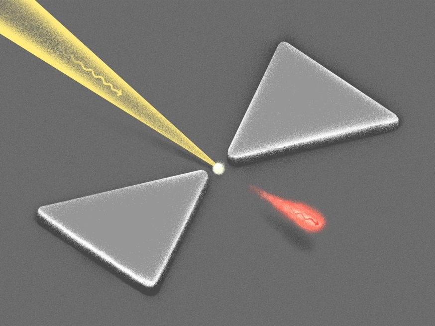
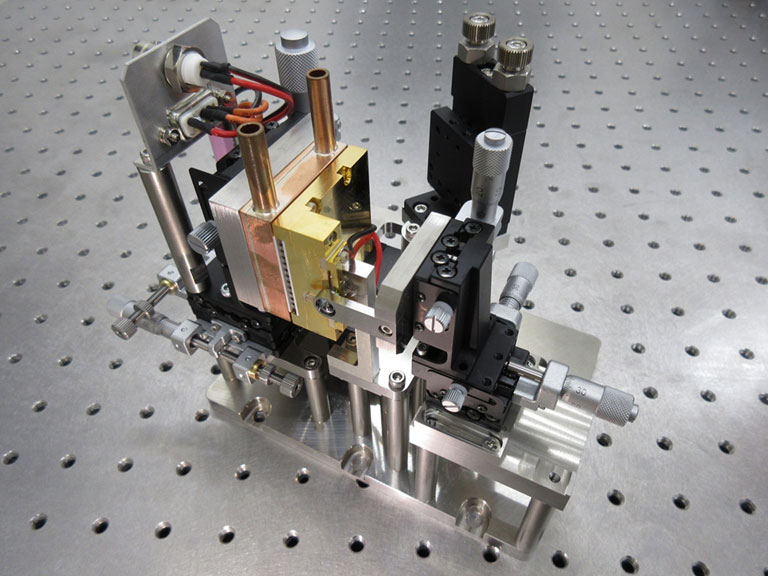
In order to send, receive, and process electromagnetic signals, antennas are used. An antenna is a device capable of effectively transmitting, picking up, and redirecting electromagnetic radiation. Typically, one thinks of antennas as macroscopic devices operating in the radio and microwave range. However, there are similar optical devices (Fig. 1). The wavelengths of visible light amount to several hundred nanometers. As a consequence, optical antennas are, by necessity, nanosized devices. Optical nanoantennas, which can focus, direct, and effectively transmit light, have a wide range of applications, including information transmission over optical channels, photodetection, microscopy, biomedical technology, and even speeding up chemical reactions.
For an antenna to pick up and transmit signals efficiently, its elements need to be resonant. In the radio band, such elements are pieces of wire. In the optical range, silver and gold nanoparticles with plasmonic resonances (Fig. 2a) have long been used for this purpose. Electromagnetic fields in such particles can be localized on a scale of 10 nanometers or less, but most of the energy of the field is wasted due to Joule heating of the conducting metal. There is an alternative to plasmonic nanoparticles, which has been studied extensively for the last five years, namely particles of dielectric materials with high refractive indices at visible light frequencies, such as silicon. When the size of the dielectric particle and the wavelength of light are just right, the particle supports optical resonances of a particular kind, called Mie resonances (Fig. 2b). Because the material properties of dielectrics are different from those of metals, it is possible to significantly reduce resistive heating by replacing plasmonic nanoantennas with dielectric analogs.
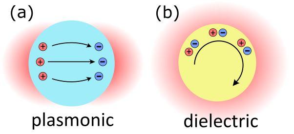
Fig. 2. Optical resonances in plasmonic (a) and dielectric (b) nanoparticles. Image courtesy of the authors of the paper.
The key characteristic of a material determining Mie resonance parameters is the refractive index. Particles made of materials with high refractive indices have resonances characterized by high quality factors. This means that in these materials electromagnetic oscillations last longer without external excitation. In addition, higher refractive indices correspond to smaller particle diameters, allowing for more miniature optical devices. These factors make high-index materials — i.e., those with high indices of refraction — more suitable for the implementation of dielectric nanoantennas.
In their paper published in Optica, the researchers systematically examine the available high-index materials in terms of their resonances in the visible and infrared spectral ranges. Materials of this kind include semiconductors and polar crystals, such as silicon carbide. To illustrate the behavior of various materials, the authors present their associated quality factors, which indicate how quickly oscillations excited by incident light die out. Theoretical analysis enabled the researchers to identify crystalline silicon as the best currently available material for the realization of dielectric antennas operating in the visible range, with germanium outperforming other materials in the infrared band. In the mid-infrared part of the spectrum, which is of particular interest due to possible applications, such as radiative cooling, i.e., the cooling of a heated body by means of radiating heat in the form of electromagnetic waves into the environment; and thermal camouflage — reducing thermal radiation given off by an object, thus making it invisible to infrared cameras, the compound of germanium and tellurium took the pedestal, Fig. 3.
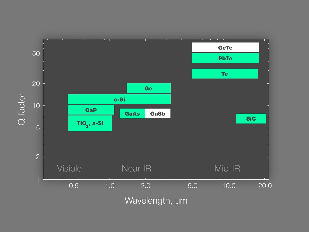
Fig. 3. Comparison of various high-index materials in terms of their quality factors, which reflect how long it takes for the Mie resonance of the particle to fade. Higher Q factors indicate longer fading times and a more pronounced resonant behavior of the particle. Image courtesy of the authors of the paper.
There are fundamental limitations on the value of the quality factor. It turns out that high refractive indices in semiconductors are associated with interband transitions of electrons, which inevitably entail the absorption of energy carried by the incident light. This absorption in turn leads to a reduction of the quality factor, as well as heating, and that is precisely what the researchers are trying to get rid of. There is, therefore, a delicate balance between a high index of refraction and energy losses.
“This study is special both because it offers the most complete picture of high-index materials, showing which of them is optimal for fabricating a nanoantenna operating in this spectral range, and because it provides an analysis of the manufacturing processes involved,” notes Dmitry Zuev, research scientist at the Metamaterials laboratory of the Faculty of Physics and Engineering, ITMO University. “This enables a researcher to select a material, as well as the desired manufacturing technique, taking into account the requirements imposed by their specific situation. This is a powerful tool furthering the design and experimental realization of a wide range of dielectric nanophotonic devices.”
According to the overview of manufacturing techniques, silicon, germanium, and gallium arsenide are the most thoroughly studied high-index dielectrics used in nanophotonics. A wide range of methods are available for manufacturing resonant nanoantennas based on these materials, including lithographic, chemical, and laser-assisted methods. However, in the case of some materials, no technology for fabrication of resonant nanoparticles has been developed. For example, researchers have yet to come up with ways of making nanoantennas from germanium telluride, whose properties in the mid-infrared range were deemed the most attractive by the theoretical analysis.
“Silicon is currently, beyond any doubt, the most widely used material in dielectric nanoantenna manufacturing,” says Denis Baranov, a PhD student at MIPT. “It is affordable, and silicon-based fabrication techniques are well established. Also, and this is important, it is compatible with the CMOS technology, an industry standard in semiconductor engineering. But silicon is not the only option. Other materials with even higher refractive indices in the optical range might exist. If they are discovered, this would mean great news for dielectric nanophotonics.”
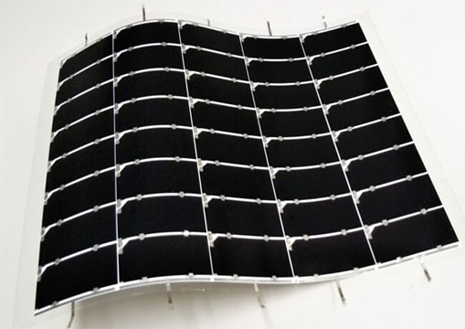
The research findings obtained by the team could be used by nanophotonics engineers to develop new resonant nanoantennas based on high-index dielectric materials. Besides, the paper suggests further theoretical and experimental work devoted to the search for other high-index materials with superior properties to be used in new improved dielectric nanoantennas. Such materials could, among other things, be used to considerably boost the efficiency of radiative cooling of solar cells, which would constitute an important technological advance.
RELATED JOURNAL ARTICLE

