JANUARY 19, 2017
Optical fibers are the backbone of modern communications, shuttling information from A to B through thin glass filaments as pulses of light. They are used extensively in telecommunications, allowing information to travel at near the speed of light virtually without loss.
These days, biologists, physicists and other scientists regularly use optical fibers to pipe light around inside their labs. In one recent application, quantum research labs have been reshaping optical fibers, stretching them into tiny tapers (see JQI News on Nanofibers and designer light traps). For these nanometer-scale tapers, or nanofibers, the injected light still makes its way from A to B, but some of it is forced to travel outside the fiber’s exterior surface. The exterior light, or evanescent field, can capture atoms and then carry information about that light-matter interaction to a detector (See JQI News on Thermometry using optical nanofibers).
Fine-tuning such evanescent light fields is tricky and requires tools for characterizing both the fiber and the light. To this end, researchers from JQI and the Army Research Laboratory (ARL) have developed a novel method to measure how light propagates through a nanofiber, allowing them to determine the nanofiber’s thickness to a precision less than the width of an atom. The technique, described in the January 20, 2017 issue of the journal Optica, is direct, fast and, unlike the standard imaging method, preserves the integrity of the fiber. As a result, the probe can be used in-situ with the nanofiber fabrication equipment, which will streamline implementation in quantum optics and quantum information experiments. Developing reliable and precise tools for this platform may enable nanofiber technology for sensing and metrology applications.
Light waves have a characteristic size called the wavelength. For visible light, the wavelength is roughly 100 times smaller than a human hair. Light can also have the appearance of different shapes, such a solid circle, ring, clover and more (see image below). Fibers restrict the way light waves can travel and twisting or bending a fiber will alter the light’s characteristics. Nanofibers are made by reshaping a normal fiber into an hourglass-like design, which further affects the guided light waves.

Examples of light shapes. Each panel shows a 3D (top) and 2D (bottom) intensity profile. The red (blue) areas indicate more (less) light intensity. The effect of the fiber appears in the 3D images as a sharp cutout; in 2D the fiber interface looks like a ring-shaped edge. (Images are calculations courtesy of P. Solano and L. Orozco)
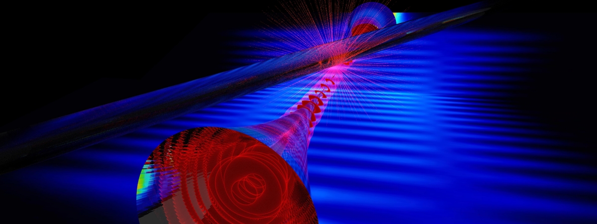
In this experiment, researchers inject a combination of light shapes into a nanofiber. The light passes down a thinning taper, squeezes through a narrow waist, and then exits out the other side of the taper. The changing fiber size distorts the light waves, and multiple patterns emerge from the interfering light shapes (See JQI News on Collecting lost light). This is analogous to musical notes, or sound waves, beating together to form a complex chord.
The researchers make direct measurements of the interference patterns (beats). To do this, they employ a second micron-sized fiber that acts as a non-invasive sensor. The nanofiber is on a moving stage and crosses the probe fiber at an oblique angle. At the touching point, a tiny fraction of nanofiber light evanescently enters the second fiber and travels to a detector. As they scan the probe along the length of the nanofiber, the probe detector collects information about the evolving patterns of nanofiber light. The researchers simultaneously monitor the light transmitting through the nanofiber to ensure that the probe process is harmless.
The team can achieve a high level of precision with this technique because they are not imaging the fiber with a camera, which would have a spatial resolution limited by the collected light’s wavelength. UMD graduate student Pablo Solano explains, “We are actually seeing the different light modes mix together and that sets the limits on determining the fiber waist—in this case sub-angstrom.” A standard tool known as scanning electron microscopy (SEM) can also measure fiber dimensions with nanoscale resolution. This, however, has a comparative disadvantage, says Eliot Fenton, a UMD undergraduate student working on the project, “With our new method, we can avoid using SEM, which destroys the fiber with imaging chemicals and heating.” Other techniques involve collecting randomly scattered light from the fiber, which is less direct and susceptible to errors. Solano summarizes how researchers can benefit from this new tool, “By directly and sensitively measuring the interference (beating) of light without destroying the fiber, we can know exactly the kind of electromagnetic field that we would apply to atoms.”
REFERENCE PUBLICATION
"Modal interference in optical nanofibers for sub-Angstrom radius sensitivity," F.K. Fatemi, J.E. Hoffman, P. Solano, E.F. Fenton, G. Beadie, S.L. Rolston, L.A. Orozco, Optica, 4, 157–162 (2017)

