7-Nov-2017
WASHINGTON -- An international team of researchers has developed a new light-based manipulation method that could one day be used to mass produce electronic components for smartphones, computers and other devices. A cheaper and faster way to produce these components could make it less expensive to connect everyday objects -- from clothing to household appliances -- to the internet, advancing the concept known as the Internet of Things. The micromanipulation technique might also be used to create a safer and faster-charging replacement for mobile device batteries.
Optical traps, which use light to hold and move small objects in liquid, are a promising non-contact method for assembling electronic and optical devices. However, when using these traps for manufacturing applications, the liquid must be removed, a process that tends to displace any pattern or structure that has been formed using an optical trap.
In The Optical Society (OSA) journal Optics Express, researchers in Steven Neale's Micromanipulation Research Group, University of Glasgow, Scotland, detail their method for using an advanced optical trapping approach known as optoelectronic tweezers to assemble electrical contacts. Thanks to an innovative freeze-drying method developed by Shuailong Zhang, a member of Neale's research group, the liquid could be removed without disturbing the assembled components.
"The forces formed by these optoelectronic tweezers have been compared to Star-Trek like tractor beams that can move objects through a medium with nothing touching them," said Neale. "This conjures up images of assembly lines with no robotic arms. Instead, discrete components assemble themselves almost magically as they are guided by the patterns of light."
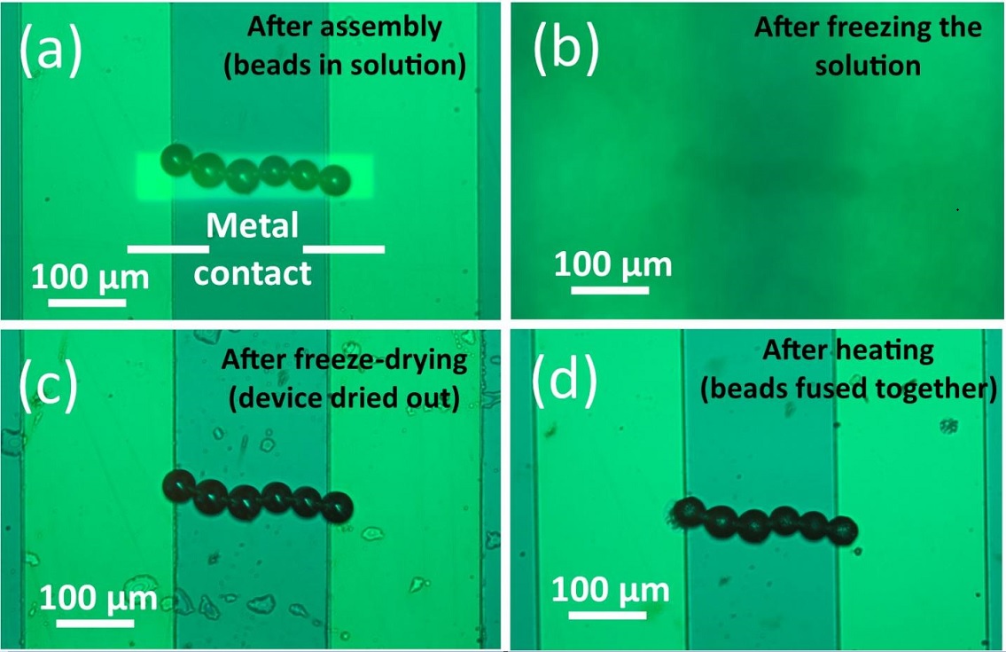
The researchers demonstrated the technique by assembling a pattern of tiny solder beads with an optoelectronic trap, removing the liquid, and then heating the pattern to fuse the beads together, forming electrical connections. They used the solder beads to demonstrate that in the future, these microparticles could be assembled and fused to create electrical connections.
"Optoelectronic tweezers are cost-effective and allow parallel micromanipulation of particles," said Zhang, who is now at the University of Toronto in Canada. "In principle, we can move 10,000 beads at the same time. Combining this with our freeze-drying approach creates a very inexpensive platform that is suitable for use in mass production."
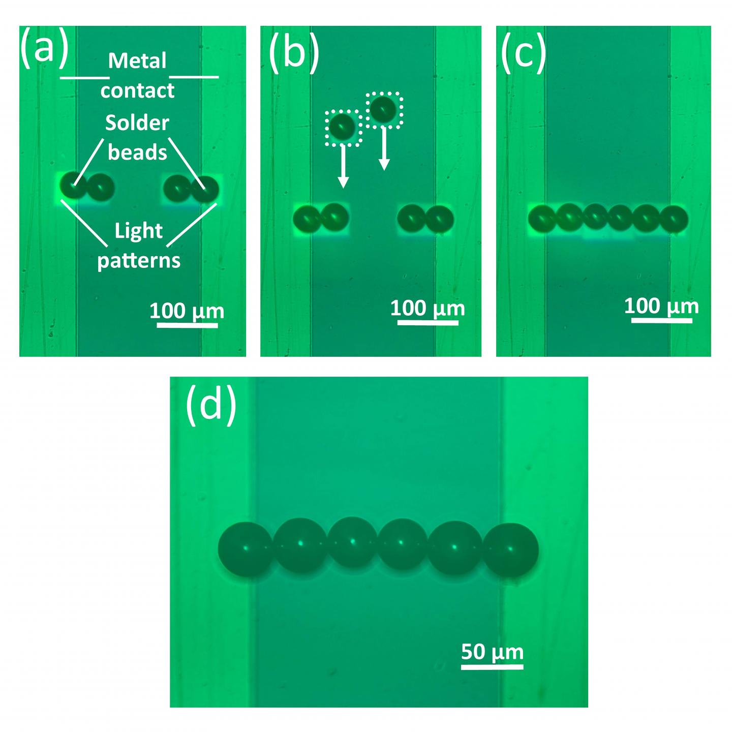
Researchers used optoelectronic tweezers to assemble a line of solder beads. By removing the liquid with a freeze-drying approach, the assembled beads stay fixed after the liquid is removed.
Credit: Shuailong Zhang
Improved electronics manufacturing
The new technique could offer an alternative way to make the circuit boards that connect the components found in most of today's electronics. These types of devices are currently made using automated machines that pick up tiny parts, place them onto the circuit board and solder them into place. This process requires an expensive motorized stage to position the board and a costly high-precision robotic arm to pick up and place the tiny parts onto the device. The cost of these micromanipulation systems continues to rise as the shrinking size of electronics increases precision requirements.
"The optoelectronic tweezers and freeze-drying technique can be used to not only assemble solder beads, but also to assemble a broad range of objects such as semiconductor nanowires, carbon nanotubes, microlasers and microLEDs," said Zhang. "Eventually, we want to use this tool to assemble electronic components such as capacitors and resistors as well as photonic devices, such as lasers and LEDs, together in a device or system."
Trapping particles with optoelectronic manipulation
The researchers used optoelectronic tweezers because this optical manipulation approach can form thousands of traps at once, offering the potential of massively parallel assembly. The tweezers are formed using a layer of silicon that changes its electrical conductivity when exposed to light. In the areas exposed to points of light, a non-uniform electric field forms that interacts with particles or beads in a liquid layer on top of the silicon, allowing the particles to be precisely moved by moving the point of light. Creating patterns of light points allows multiple particles to be moved simultaneously.
"Using our method, we can move solder beads measuring from the nanometer range up to about 150 microns," said Zhang. "We have been able to move objects that are over 150 microns, but it's more challenging because as the size of the object increases, the frictional force also increases."
After using the optoelectronic tweezers to assemble a pattern of 40-micron-diameter, commercially available solder beads, the researchers froze the liquid in the optoelectronic tweezer device and then reduced the surrounding pressure to allow the frozen liquid to turn from a solid directly into a gas. This freeze-drying approach allowed the assembled solder beads to remain fixed in place after the liquid was removed. The researchers say it can be used to remove liquid used with any type of optical trap, or even traps formed with acoustic waves.
In addition to assembling the solder beads into different lines, the researchers also demonstrated parallel assembly of several beads and used the beads to form electrical connections. The solder beads exhibit a strong dielectric force, which means they can be moved accurately and fast, allowing very efficient assembly of structures.
The researchers are now working to turn their laboratory-based system into one that would combine the optoelectronic tweezer and freeze-drying process in a single unit. They are also developing a software interface to control the generation of a light pattern based on the number of particles that needed to be trapped.
"We are now using a computer to generate the light pattern to move the beads, but we are working on an app that would allow a tablet or smart phone to be used instead," said Zhang. "This could allow someone to sit away from the system and use their finger to control the movements of the particles, for example."
Neale recently received funding to continue this line of research by using the new optical micromanipulation approach to create high energy density capacitors to replace batteries in mobile devices.
###
Paper: S. Zhang, Y. Liu, Y. Qian, W. Li, J. Juvert, P. Tian, J.-C. Navarro, A.W. Clark, E. Gu, M.D. Dawson, J.M. Cooper, S.L. Neale, "Manufacturing with light - micro-assembly of opto-electronic microstructures," Opt. Express, Volume 25, Issue 23, 28838-28850 (2017). DOI: 10.1364/OE.25.028838.

