January 21, 2016
By Andy Fell
For hundreds of years, the general design of an optical telescope has remained pretty much the same. Even if you’re looking at the stars with the naked eye, the image-forming process works in a similar way. Both methods collect light from an object and refract that light to form an image.
Now researchers at the University of California, Davis, are working with Lockheed Martin to develop a radically new kind of telescope that will be much lighter and smaller, both of which are important considerations especially for instruments to be launched into space.
“We can only scale the size and weight of telescopes so much before it becomes impractical to launch them into orbit and beyond,” said Danielle Wuchenich, senior research scientist at Lockheed Martin’s Advanced Technology Center in Palo Alto, California. “Besides, the way our eye works is not the only way to process images from the world around us.”
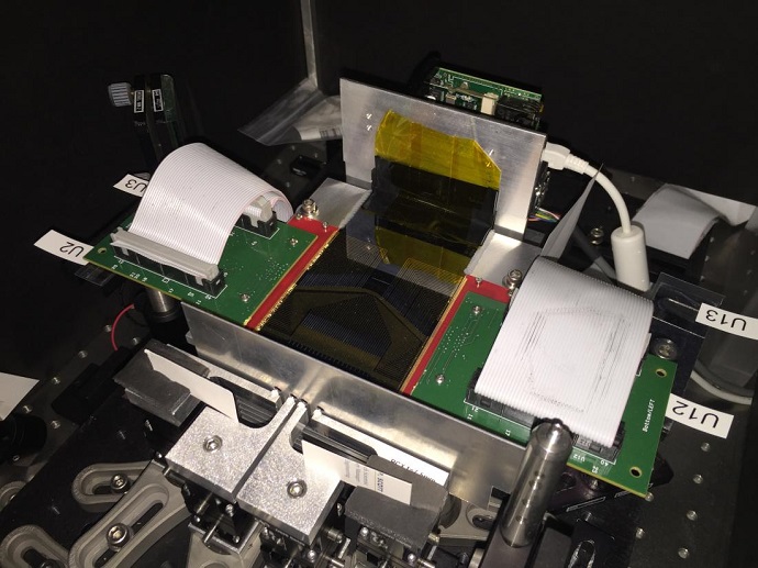
Lockheed Martin’s SPIDER (Segmented Planar Imaging Detector for Electro-optical Reconnaissance) concept trades bulky lenses and telescopes for a thin layer of hundreds or thousands of tiny lenses that feed photonic integrated circuits on silicon chips. These photonic circuits, developed by Professor Ben Yoo and his team at UC Davis’ Department of Electrical and Computer Engineering, combine the light from pairs of lenses to construct a digital image from the interference fringes caused by overlapping waves.
SPIDER eyes: Power in numbers
Interference fringes appear when waves coming from the same source through slightly different routes overlap. Think about ripples spreading in a pond. Where peaks or troughs coincide, they reinforce each other; where a peak meets a trough, they cancel out. When the waves originally came from the same source, the resulting interference patterns can yield information about their original state.
Large-scale astronomical interferometer arrays are already used to form ultra-high-resolution images of objects in space from optical and radio telescopes. The goal of SPIDER is to shrink that concept to a thin layer of thousands of lenses feeding silicon chips that can process photons.
UC Davis photonic technology
Yoo’s laboratory works on various devices and circuits that use light for ultra-high-capacity image processing, computing and networking. He was initially approached by Lockheed Martin about the SPIDER project at the recommendation of DARPA, the Defense Advanced Research Projects Agency, which has funded a number of research projects in Yoo’s laboratory.
For the SPIDER project, “we’ve fabricated a chip that can collect the fringes and form images in three bands of wavelengths,” Yoo said. Behind each lens are multiple waveguides that gather light from a wider field of view. Each pair of waveguides at a given band of wavelengths will form fringes. The amplitude and phase of the fringes will be processed to construct a digital image for each color.
A thin, photonic integrated circuit containing many waveguides together with many miniature lenses can create high resolution images without resorting to a large telescope structure such as Hubble telescope, Yoo said.
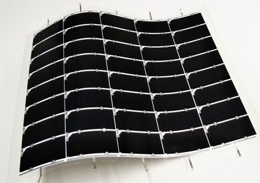
Much as thin displays have replaced bulky old television sets, SPIDER imaging technology could reduce the size, weight and power needs for telescopes by 10 to 100-fold. That could make a big difference for commercial and government satellites alike. The technology also promises to be more robust and flexible than complex lenses and mirrors.
The future looks bright (and light)
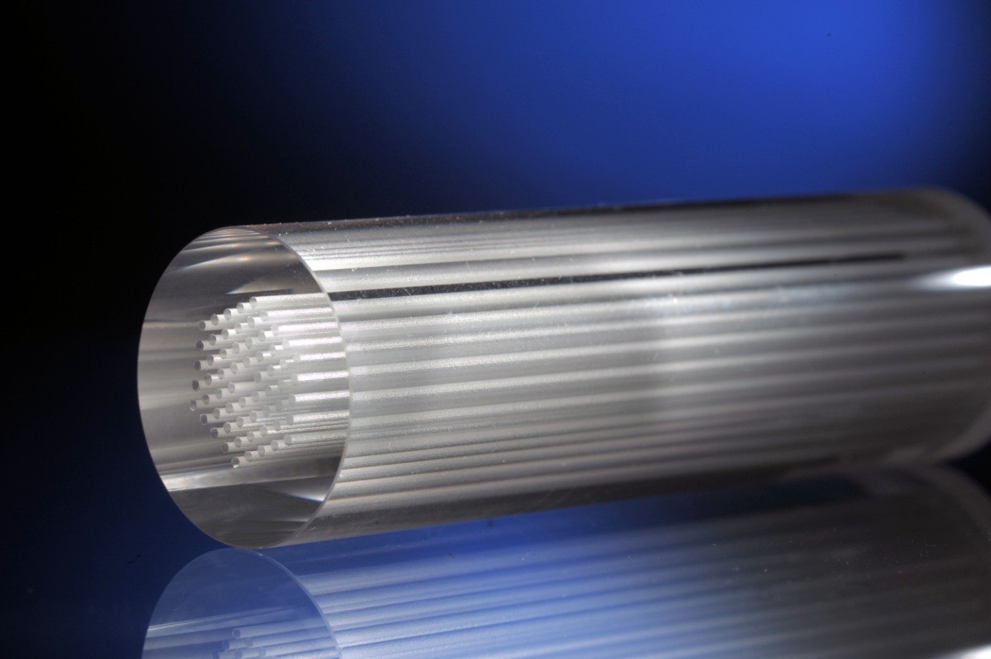
Yoo’s team fabricated their prototype photonic chips with facilities at the UC Davis College of Engineering’s Center for Nano-MicroManufacturing. The next generation of chips will be built with three-dimensional laser inscription — using an ultrafast laser to write waveguides of any shape within a solid piece of glass, using apparatus developed in Yoo’s lab.
While the SPIDER prototype today is still in its early stages with less than 100 waveguides, Yoo expects that the new generation of photonic integrated circuits created by three-dimensional laser inscription will enable highly functional and densely integrated systems.
Large-scale manufacturing of such photonic integrated circuits based on UC Davis’ technologiescan leverage a newly launched institute, the American Institute for Manufacturing Integrated Photonics (AIM Photonics). UC Davis is one of the Tier-1 members of AIM Photonics, a partnership between industry, universities and government agencies formally announced by Vice President Joe Biden in July 2015. The goal of the institute is to create a national manufacturing infrastructure for photonic integrated circuits, widely accessible and inherently flexible to meet the challenges of the marketplace with practical, innovative solutions.

