June 13, 2016
David L. Chandler | MIT News Office
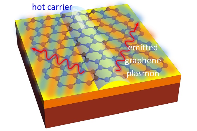
When an airplane begins to move faster than the speed of sound, it creates a shockwave that produces a well-known “boom” of sound. Now, researchers at MIT and elsewhere have discovered a similar process in a sheet of graphene, in which a flow of electric current can, under certain circumstances, exceed the speed of slowed-down light and produce a kind of optical “boom”: an intense, focused beam of light.
This entirely new way of converting electricity into visible radiation is highly controllable, fast, and efficient, the researchers say, and could lead to a wide variety of new applications. The work is reported today in the journal Nature Communications, in a paper by two MIT professors — Marin Soljačić, professor of physics; and John Joannopoulos, the Francis Wright Davis Professor of physics — as well as postdoc Ido Kaminer, and six others in Israel, Croatia, and Singapore.
The new finding started from an intriguing observation. The researchers found that when light strikes a sheet of graphene, which is a two-dimensional form of the element carbon, it can slow down by a factor of a few hundred. That dramatic slowdown, they noticed, presented an interesting coincidence. The reduced speed of photons (particles of light) moving through the sheet of graphene happened to be very close to the speed of electrons as they moved through the same material.
“Graphene has this ability to trap light, in modes we call surface plasmons,” explains Kaminer, who is the paper’s lead author. Plasmons are a kind of virtual particle that represents the oscillations of electrons on the surface. The speed of these plasmons through the graphene is “a few hundred times slower than light in free space,” he says.
This effect dovetailed with another of graphene’s exceptional characteristics: Electrons pass through it at very high speeds, up to a million meters per second, or about 1/300 the speed of light in a vacuum. That meant that the two speeds were similar enough that significant interactions might occur between the two kinds of particles, if the material could be tuned to get the velocities to match.
That combination of properties — slowing down light and allowing electrons to move very fast — is “one of the unusual properties of graphene,” says Soljačić. That suggested the possibility of using graphene to produce the opposite effect: to produce light instead of trapping it. “Our theoretical work shows that this can lead to a new way of generating light,” he says.
Specifically, he explains, “This conversion is made possible because the electronic speed can approach the light speed in graphene, breaking the ‘light barrier.’” Just as breaking the sound barrier generates a shockwave of sound, he says, “In the case of graphene, this leads to the emission of a shockwave of light, trapped in two dimensions.”
The phenomenon the team has harnessed is called the Čerenkov effect, first described 80 years ago by Soviet physicist Pavel Čerenkov. Usually associated with astronomical phenomenon and harnessed as a way of detecting ultrafast cosmic particles as they hurtle through the universe, and also to detect particles resulting from high-energy collisions in particle accelerators, the effect had not been considered relevant to Earthbound technology because it only works when objects are moving close to the speed of light. But the slowing of light inside a graphene sheet provided the opportunity to harness this effect in a practical form, the researchers say.
There are many different ways of converting electricity into light — from the heated tungsten filaments that Thomas Edison perfected more than a century ago, to fluorescent tubes, to the light-emitting diodes (LEDs) that power many display screens and are gaining favor for household lighting. But this new plasmon-based approach might eventually be part of more efficient, more compact, faster, and more tunable alternatives for certain applications, the researchers say.
Perhaps most significantly, this is a way of efficiently and controllably generating plasmons on a scale that is compatible with current microchip technology. Such graphene-based systems could potentially be key on-chip components for the creation of new, light-based circuits, which are considered a major new direction in the evolution of computing technology toward ever-smaller and more efficient devices.
“If you want to do all sorts of signal processing problems on a chip, you want to have a very fast signal, and also to be able to work on very small scales,” Kaminer says. Computer chips have already reduced the scale of electronics to the points that the technology is bumping into some fundamental physical limits, so “you need to go into a different regime of electromagnetism,” he says. Using light instead of flowing electrons as the basis for moving and storing data has the potential to push the operating speeds “six orders of magnitude higher than what is used in electronics,” Kaminer says — in other words, in principle up to a million times faster.
One problem faced by researchers trying to develop optically based chips, he says, is that while electricity can be easily confined within wires, light tends to spread out. Inside a layer of graphene, however, under the right conditions, the beams are very well confined.
“There’s a lot of excitement about graphene,” says Soljačić, “because it could be easily integrated with other electronics” enabling its potential use as an on-chip light source. So far, the work is theoretical, he says, so the next step will be to create working versions of the system to prove the concept. “I have confidence that it should be doable within one to two years,” he says. The next step would then be to optimize the system for the greatest efficiency.
This finding “is a truly innovative concept that has the potential to be the key toward solving the long-standing problem of achieving highly efficient and ultrafast electrical-to-optical signal conversion at the nanoscale,” says Jorge Bravo-Abad, an assistant professor at the Autonomous University of Madrid, in Spain, who was not involved in this work.
In addition, Bravo-Abad says, “the novel instance of Čerenkov emission discovered by the authors of this work opens up whole new prospects for the study of the Čerenkov effect in nanoscale systems, without the need of sophisticated experimental set-ups. I look forward to seeing the significant impact and implications that these findings will surely have at the interface between physics and nanotechnology.”
The research was supported by the U.S. Army Research Laboratory and the U.S. Army Research Office, through the Institute for Soldier Nanotechnologies at MIT. The team included researchers Yichen Shen, Ognjen Ilic, and Josue Lopez at MIT; Yaniv Katan at Technion, in Haifa, Israel; Hrvoje Buljan at the University of Zagreb in Croatia; and Liang Jie Wong at the Singapore Institute of Manufacturing Technology.
Paper: “Efficient plasmonic emission by the quantum Čerenkov effect from hot carriers in graphene.”

