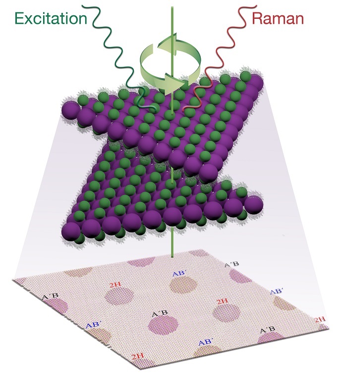
OAK RIDGE, Tenn., March 2, 2016 – Stacking layers of nanometer-thin semiconducting materials at different angles is a new approach to designing the next generation of energy-efficient transistors and solar cells. The atoms in each layer are arranged in hexagonal arrays. When two layers are stacked and rotated, atoms from one layer overlap with those in the other layer and can form an infinite number of overlapping patterns, like the Moiré patterns that result when two screens are overlaid and one is rotated on top of the other. Theoretical calculations predict excellent electronic and optical properties for some stacking patterns, but practically, how can these patterns be made and characterized?
Recently a team led by researchers from the Department of Energy’s Oak Ridge National Laboratory used the vibrations between two layers to decipher their stacking patterns. The team employed a method called low-frequency Raman spectroscopy to measure how the layers vibrate with respect to each other and compared the frequencies of the measured vibrations with their theoretically predicted values. Their study provides a platform for engineering two-dimensional (2D) materials with optical and electronic properties that strongly depend on stacking configurations. The findings are published in ACS Nano, a journal of the American Chemical Society.
“Low-frequency Raman spectroscopy, in combination with first-principles modeling, offers a quick and easy approach to reveal complex stacking configurations in the twisted bilayers of a promising semiconductor, without relying on other expensive and time-consuming experimental techniques,” said co-lead author Liangbo Liang, a Wigner Fellow at ORNL. “We are the first to show that low-frequency Raman spectra can be used as fingerprints to characterize the relative layer stacking in semiconducting 2D materials.”
In Raman scattering, an optical method for probing atomic vibrations, a material scatters monochromatic light from a laser. Whereas conventional Raman spectroscopy may probe more than approximately 3 trillion atomic vibrations per second, low-frequency Raman spectroscopy detects vibrations that are an order of magnitude slower. The low-frequency technique is sensitive to weak attractive forces between layers, called van der Waals coupling. It can provide crucial insight about layer thickness and stacking—aspects that govern fundamental properties of 2D materials.
“This work combines state-of-the art synthesis and processing of 2D materials, their unique spectroscopic characterization, and data interpretation using first-principles theory,” said co-lead author Alex Puretzky. “High-resolution Raman spectroscopy that can probe low-frequency modes requires specialized instrumentation, and only a few places around the world have such a capability together with advanced synthesis and characterization tools, and theory and computational modeling expertise. The Center for Nanophase Materials Sciences at ORNL is among them.”
Chemical vapor deposition, widely employed to synthesize 2D materials like graphene, was used to make perfectly triangular crystal monolayers of molybdenum diselenide just three atoms thick. Feedstock molecules of molybdenum oxide and sulfur were reacted in a flowing gas within a high-temperature furnace to form the triangular crystals on silicon substrates.
“Numerous parameters need to be properly adjusted to synthesize large, triangular 2D crystals successfully,” Puretzky said. “Then, carefully removing the crystals and stacking them precisely in different orientations is a big challenge.”
He continued, “The precise, equilateral triangular shape of the synthesized and transferred crystals allowed us to measure the twist angles with a high precision using standard optical and atomic force microscopy images, which was a key factor in our experiments.”
Theoretical and computational aspects were challenging too. “Raman spectroscopy is heavily based on theory for interpretation and assignment of the observed Raman spectra, especially for new materials that have never before been measured,” Puretzky said.
The study revealed patterns in the stacked bilayers that strongly depend on the twist angle. Some specific twist angles, though, showed periodically repeating patches with the same stacking orientation. “These unique patterns may provide a new platform for optoelectronic applications of these materials,” Puretzky said.
The team’s findings also showed fascinating effects of the vibrations between the layers. As different stacking patterns appeared when layers were displaced, variable spacings occurred between the layers at some specific twist angles. The researchers plan further measurements and modeling for different stacking configurations to better understand how these vibrational decays might alter the thermal properties of these materials—knowledge that could affect applications in heat dissipation and thermoelectric energy conversion.
The title of the paper is “Twisted MoSe2 Bilayers with Variable Local Stacking and Interlayer Coupling Revealed by Low-Frequency Raman Spectroscopy.”
Raman spectroscopy, including aspects of theory, was conducted at the Center for Nanophase Materials Sciences, a DOE Office of Science User Facility at ORNL. Synthesis, including chemical vapor deposition, was supported by the DOE Office of Science. At Rensselaer Polytechnic Institute, theoretical work was supported by the National Science Foundation, and computations used resources of the Center for Computational Innovation.
UT-Battelle manages ORNL for DOE’s Office of Science. The single largest supporter of basic research in the physical sciences in the United States, the Office of Science is working to address some of the most pressing challenges of our time.—by Dawn Levy

