June 07, 2016
WASHINGTON — Researchers have created a new optical lens that is flat, rather than curved like traditional glass lenses. The unique optical properties available from the flat lens could help reduce the size of computer hard drives and create exceptionally small microscopes, among other applications.
“We've shown a new way to control light,” said Ruben Maas, who carried out the research in Albert Polman’s research group at the Center for Nanophotonics, FOM Institute AMOLF, The Netherlands. “This new type of optical element will hopefully enable new types of optical devices that are much smaller than what we've seen up until now.”
In The Optical Society's journal for high impact research,Optica, the researchers detail the fabrication and characterization of their new lens, which is made of extremely thin layers of silver and titanium dioxide. The flat lens offers properties not available from traditional lenses including a larger field of view and a very short working distance that allows it to be placed very close to an object of interest.
Building a flat lens
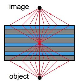
Traditional lenses use curved glass to force light to converge or focus. The key to the team’s new flat lens is alternating layers of silver and titanium dioxide. It may seem counterintuitive to use silver to form a lens, since metals tend to act like a mirror by reflecting all the light hitting the surface. However, for very thin layers of metal — thinner than the wavelength of light — a portion of the light will transmit through the material. This transmitted light undergoes an unusual phenomenon called negative refraction that allows the silver and titanium dioxide layers to act as a lens, focusing light coming from many directions.
The researchers created the thin layers of silver and titanium dioxide using physical vapor deposition, a method commonly used in industrial settings to create coatings or protective layers. The difficult task was optimizing the layer thicknesses with sub-nanometer precision. The researchers found that a 10-layer structure alternating between 53.2-nanometer (nm) thick layers of silver and 25.0-nm thick layers of titanium dioxide produced the best flat lens.
Maas and his colleagues made a lens that operates in the ultraviolet (UV) part of the spectrum because silver and titanium dioxide show low optical absorption in the UV and because this wavelength produces a higher resolution. However, other materials can be used to create a flat lens that works at other wavelengths. “The resolution we can achieve is still bound by the diffraction limit of light, which scales with the wavelength,” said Maas. “The short UV wavelength automatically gives it higher resolution than for visible light.”
Small optics make small devices
The new flat lens could be very useful for lab-on-a-chip devices, which integrate several laboratory processes onto a chip that is up to a few square centimeters in size. Many of the processes performed by these devices require optical signals, but it is challenging to fabricate a curved lens small enough to integrate into these devices, and it can be difficult to maintain the necessary optical alignment. A flat lens could more easily fit the size requirements, and because it can focus light coming from a range of angles, up to 55 degrees from normal, it wouldn’t require precise alignment.
The new flat lens could also be used with optical recording techniques such as magneto-optical recording or heat-assisted magnetic recording to allow even more information storage in a smaller space in computer hard drives.
The researchers are also examining the possibility of tuning the optical properties of the lens using an electrical signal, which could bring promising applications in telecommunications. “Information is transmitted through optical fibers with optical signals,” said Maas. “Connecting this optical signal to an electrical signal, or imprinting an electrical signal onto an optical signal is a relatively slow and tedious process at the moment, but we envision that a flat lens could be used for electro-optical coupling by applying a voltage over the multilayer structure, which then modulates the transmission.”
Creating an image
In the paper, the researchers show that their flat lens produced a clear image of a 100 nm slit placed about 350 nm from the lens. Although the demonstration lens had lateral dimensions of 25x25 microns, the researchers say that it could easily be enlarged to centimeters or more.
“By applying the multilayer structure over a very large surface, it acts as a lens over this entire surface,” said Maas. “In a normal microscope you would have to scan across the sample to image it because the field of view is so limited. With a large-diameter flat lens, scanning wouldn’t be necessary because the field of view would be as large as the lens.”
The lens does show significant loss of light due to reflection, but the ability to use it in ways that are impossible for traditional lenses – such as on a very small scale, where alignment is critical, or very close to the object – will override this drawback for those applications.
The researchers previously designed a similar flat lens where all the titanium oxide layers were of equal thickness but the metal layer alternated between thinner and thicker layers. “We figured out that we actually don't need to fabricate the lens in this complicated manner,” said Maas. “In this paper we present a geometry where the thickness of the metal and the titanium dioxide layers are different, but all the metal layers have the same thickness and all the titanium dioxide layers have the same thickness. You can achieve exactly the same result with this more simple design.”
Paper: R. Maas, J. van de Groep, A. Polman, "Planar metal/dielectric single-periodic multilayer UV flat lens," Optica, 3, 6, 592 (2016). DOI: 10.1364/optica.3.000592.

