October 24, 2016
NICT has succeeded in the development of flexible optical design method for superconducting nanowire single-photon detectors (SSPDs or SNSPDs).
This technique enables SSPDs with a broadband high detection efficiency reject a specific wavelength, and is effective for multidisciplinary applications in fields such as the quantum cryptography, fluorescence spectroscopy, and remote sensing that require high efficiency over a precise spectral range and strong signal rejection at other wavelengths.
This achievement appeared in the “Scientific Reports” (Nature Publishing Group) on October 24, 2016. The reported results have been partially obtained as a part of JST-SENTAN program and AMED-SENTAN program from April 2015.
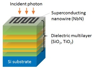
The researchers have developed SSPDs on dielectric multilayers and their optical design method, which enable them to design a variety of wavelength dependences of optical absorptance by optimizing the dielectric multilayer.
In order to achieve the high detection efficiency in SSPDs, it is crucial to optimize the optical absorptance for a target wavelength. In the conventional SSPDs, a simple cavity structure consisting of dielectric resonant layers with a mirror layer has been used. This structure is relatively simple and can effectively achieve high absorptance at the target wavelength, and the wavelength dependencies of absorptance show a single peak structure. However, in this structure, it is difficult to realize the SSPDs with high efficiency over a carefully controlled spectral range, with rejection at other wavelengths to reduce the noises.
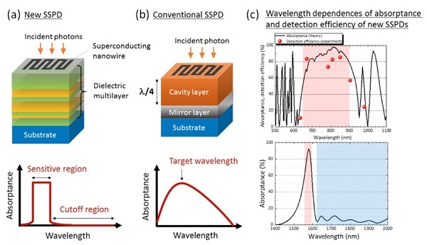
Figure 1: New and conventional SSPD structure and wavelength dependences of the absorptance and the detection efficiency.
Figure 1(a) and 1(b) show the device structures and schematics of the wavelength dependences of the absorptance for a new SSPD and a conventional one, respectively. In the simple cavity structure of the conventional SSPD (Fig. 1(b)), the optical absorptance can be enhanced by tuning the thickness of the cavity layer to the quarter of the target wavelength. However, in this structure it is difficult to design the entire region of the wavelength dependence. On the other hand, in the new SSPD structure, one can design the wavelength dependence of the absorptance flexibly by optimizing the total layer number and the thicknesses of the each layer in the dielectric multilayer. For example, the broadband high absorptance or the filter function with a cutoff wavelength can be realized in the new SSPD.
Figure 1(c) indicates the example of the wavelength dependence for the new SSPD structure. A black curve in the top figure shows the simulation result by optimizing the absorptance for the wavelengths of 650 – 900 nm. As shown in the figure, it was confirmed that the measured detection efficiency (red symbols) followed the simulation curve well. The bottom figure shows another simulated example optimized for the high absorptance at telecom wavelength with a cutoff region over 1600 nm. In this design, it is expected that external noise due to the light with the longer wavelength over 1600 nm can be reduced with the high detection efficiency for telecom wavelength.
By adopting a new SSPD structure with dielectric multilayers, it became possible to design desired wavelength dependences of the optical absorptance. As materials of dielectric multilayer, silicon dioxide (SiO2) and titanium oxide (TiO2) were used, and the niobium nitride (NbN) superconducting nanowire was put on the dielectric multilayer. The wavelength dependences of the optical absorptance in the nanowire could be designed by optimizing the layer number and thicknesses of each layer in the dielectric multilayer. They developed the SSPDs based on the optimized design, and experimentally demonstrated that the wavelength dependences of the detection efficiency follow the calculated results well. Regarding the optical design method, in order to optimize the wavelength dependence of the absorptance effectively, they performed two-step simulation of the optical multilayer calculation and the finite element analysis.
In support of the SSPD measurements, the NICT team collaborated with Osaka University, Japan and the University of Glasgow, Scotland through the NICT internship scheme.
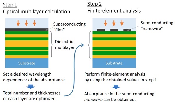
Figure 2: Two-step calculation for the wavelength dependence of the optical absorptance.
Figure 2 shows a two-step calculation for the optimization of dielectric multilayer. In the step 1, we optimized the dielectric multilayer design to realize a desired wavelength dependence of the absorptance in the superconducting film by using optical multilayer simulation software. Although the optimization process can be finished in a relatively short calculation time, the active area of SSPDs consists of a superconducting nanowire, not film. It is possible to show the different wavelength dependences of the nanowire from that of the unpatterned film even on the same dielectric multilayer design. Thus, in the step 2, we performed finite-element analysis for nanowire structure with dielectric multilayer by using the design values obtained in the step 1, and finally we confirmed that actual SSPD showed the desired wavelength dependence.
Future Prospects
The developed SSPD with the dielectric multilayer and the optical design method can be applied for wide wavelength region between ultraviolet and mid-infrared, and thus provides an important basis for development of application of SSPD to quantum cryptography, fluorescence spectroscopy, and remote sensing.
Journal Information
Journal: Scientific Reports, DOI: 10.1038/srep35240
URL: http://www.nature.com/srep/
Title: Superconducting nanowire single-photon detectors with non-periodic dielectric multilayers
Authors: Taro Yamashita, Kentaro Waki, Shigehito Miki, Robert A. Kirkwood, Robert H. Hadfield, and Hirotaka Terai

