Apr. 15, 2016
by David Salisbury
A future generation of atomically thin optoelectronics devices, including transistors, photodetectors and solar cells, is a step closer because of an advance in the art of epitaxy made by scientists at Oak Ridge National Laboratory (ORNL) with an assist from a pair of Vanderbilt physicists.
Epitaxy, the process of growing layers of crystalline film on crystalline surfaces, is a mainstay of the semiconductor manufacturing process that is at the heart of the digital revolution. Its incredible success has come about despite the fact that the variety of materials that can be grown together in this fashion has been highly limited. Only crystalline materials with nearly identical atomic structures bond in a way that makes them suitable for electronic devices.
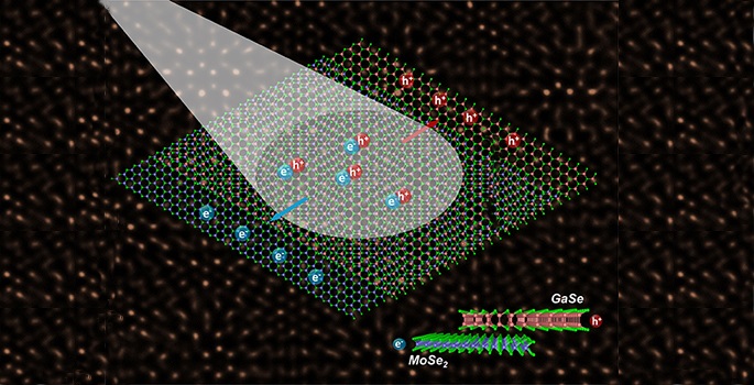
Now, however, the ORNL team has managed to take two-dimensional monolayers of two semiconductors with mismatched lattices and stack them together to form an atomically thin solar cell. The achievement demonstrates the promise of synthesizing mismatched layers to produce entire new families of functional, ultrathin optoelectronic materials. The results were published Apr. 15 in the journal Science Advances.
“This achievement is yet another demonstration of the promise of two-dimensional materials – just one atom thick – yielding devices for future applications in the real world,” said Sokrates Pantelides, William A. and Nancy F. McMinn Professor in Physics at Vanderbilt University. He and Vanderbilt University Ph.D. student Junhao Lin collaborated in the study.
ORNL News release: ‘Odd couple’ monolayer semiconductors align to advance optoelectronics

