26.11.2015
Silicon, a semiconducting material, reveals new talents when reduced to nanoscopic dimensions. A joint team at the HZB Institute of Nanoarchitectures for Energy Conversion and the Max Planck Institute for the Science of Light (MPL) has demonstrated this. Silicon nanocones generate 200 times as much infrared luminescence as comparably sized nanocolumns when excited by visible light. Modelling and experimental results show that due to their geometry, cones are able to sustain what is referred to as whispering gallery modes at infrared wavelengths which can intensify the silicon luminescence. New applications are conceivable, including silicon-based nanolasers.
Silicon is a conventional material for computer chips and solar cells. However, even though the properties of silicon are well known, nanostructures still offer up surprises. A team headed by Prof. Silke Christiansen at the HZB Institute of Nanoarchitectures for Energy Conversion together with the Max Planck Institute for the Science of Light (MPL) has shown for the first time how light behaves in a silicon nanocone. Their numerical simulations and experiments now demonstrate why this tapered geometry is able to emit optically excited luminescence a great deal better that comparably sized nanocolumns. “The cones function like arrays of tiny whispering galleries – not for sound, but rather for light”, explains Sebastian Schmitt, first author.
![]()
Nanostructures of silicon shown in scanning electron microscope image. The diameter of the nanocolumns is 570 nm. By comparison, the nanocones taper from their upper diameter of 940 nm down to 360 nm at their base. Credit: MPL
Strong luminescence in nanocones
Schmitt and his colleague George Sarau irradiated individual silicon nanocolumns and nanocones using red laser light (660 nanometres) and measured the radiation that was subsequently emitted as luminescence by the sample. It is known that luminescence in silicon (without any nanostructuring) is normally very low because excited electrons hardly recombine radiatively in this material (indirect band gap). In contrast, the nanostructures convert a much greater portion of the incident light into electromagnetic radiation in the near-infrared region. This effect in nanocones is 200 times stronger than in nanocolumns. “This is the highest luminescence gain ever measured in a silicon structure”, says Schmitt.
Whispering gallery modes
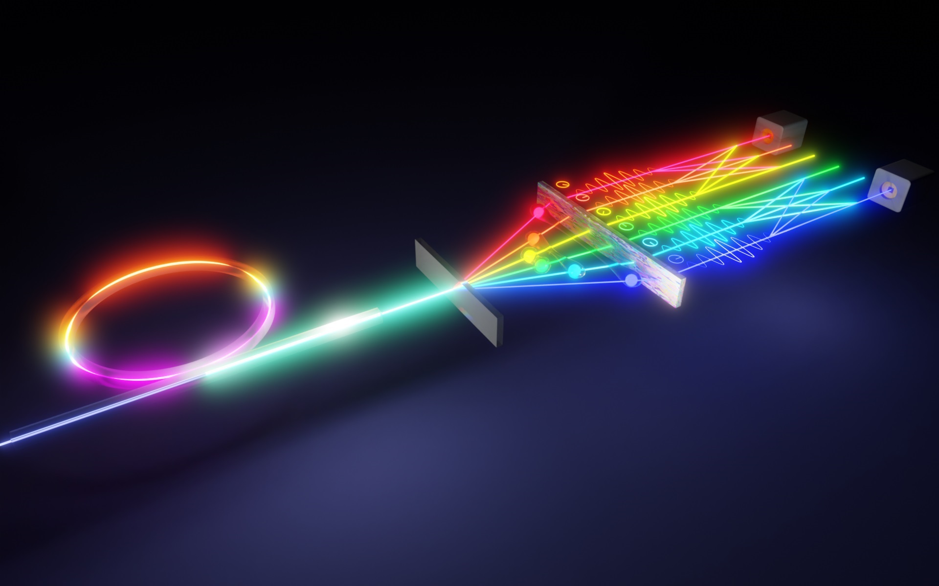
The team can also explain why this is. The propagation of electromagnetic waves in various geometries of silicon nanowires can be calculated using numerical modelling. Because the diameter of the nanocone changes with height, there are several levels at which the infrared light is constructively superposed to form standing waves. This amplification facilitates increased excitation of electrons and thus the release of luminescence. This phenomenon is known as the Purcell Effect in the field. If a light source is located in an optical resonator, spontaneous emission of light increases. The nanocones act as outstanding resonators, like optical whisper galleries for light.
![]()
The energy density of the light (1027 nm) in cross sections of the nanostructures can be numerically modelled. Whispering gallery modes only arise in nanocones. The luminescence is amplified 200 times more in nanocones than in nanocolumns.
Credit: MPL
Design rules for novel devices
“These types of nanostructures made of individual cones are not difficult to fabricate”, explains Schmitt. They would be easily integrated as new components into predominant CMOS semiconductor fabrication techniques used for diodes, optoelectronic switches, and optical sensors, for example. These structures could even produce laser light in conjunction with a suitable optically active medium, the physicist surmises. “We can derive simple design rules for semiconductor nanostructures with this kind of knowledge to exert control over the number and wavelengths of hosted modes and thereby control the luminescence”, says Christiansen.
The results have been published in the renowned Journal Scientific Reports, DOI: 10.1038/srep17089
"Observation of strongly enhanced photoluminescence from inverted cone-shaped silicon nanostuctures"
Sebastian W. Schmitt, George Sarau & Silke Christiansen

