January 9, 2015
Larry Hardesty | MIT News Office
A team of researchers has built an array of light detectors sensitive enough to register the arrival of individual light particles, or photons, and mounted them on a silicon optical chip. Such arrays are crucial components of devices that use photons to perform quantum computations.
Single-photon detectors are notoriously temperamental: Of 100 deposited on a chip using standard manufacturing techniques, only a handful will generally work. In a paper appearing today in Nature Communications, the researchers at MIT and elsewhere describe a procedure for fabricating and testing the detectors separately and then transferring those that work to an optical chip built using standard manufacturing processes.
In addition to yielding much denser and larger arrays, the approach also increases the detectors’ sensitivity. In experiments, the researchers found that their detectors were up to 100 times more likely to accurately register the arrival of a single photon than those found in earlier arrays.
“You make both parts — the detectors and the photonic chip — through their best fabrication process, which is dedicated, and then bring them together,” explains Faraz Najafi, a graduate student in electrical engineering and computer science at MIT and first author on the new paper.
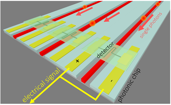
Illustration of superconducting detectors on arrayed waveguides on a photonic integrated circuit for detection of single photons.
Credit: F. Najafi/ MIT
Thinking small
According to quantum mechanics, tiny physical particles are, counterintuitively, able to inhabit mutually exclusive states at the same time. A computational element made from such a particle — known as a quantum bit, or qubit — could thus represent zero and one simultaneously. If multiple qubits are “entangled,” meaning that their quantum states depend on each other, then a single quantum computation is, in some sense, like performing many computations in parallel.
With most particles, entanglement is difficult to maintain, but it’s relatively easy with photons. For that reason, optical systems are a promising approach to quantum computation. But any quantum computer — say, one whose qubits are laser-trapped ions or nitrogen atoms embedded in diamond — would still benefit from using entangled photons to move quantum information around.
“Because ultimately one will want to make such optical processors with maybe tens or hundreds of photonic qubits, it becomes unwieldy to do this using traditional optical components,” says Dirk Englund, the Jamieson Career Development Assistant Professor in Electrical Engineering and Computer Science at MIT and corresponding author on the new paper. “It’s not only unwieldy but probably impossible, because if you tried to build it on a large optical table, simply the random motion of the table would cause noise on these optical states. So there’s been an effort to miniaturize these optical circuits onto photonic integrated circuits.”
The project was a collaboration between Englund’s group and the Quantum Nanostructures and Nanofabrication Group, which is led by Karl Berggren, an associate professor of electrical engineering and computer science, and of which Najafi is a member. The MIT researchers were also joined by colleagues at IBM and NASA’s Jet Propulsion Laboratory.
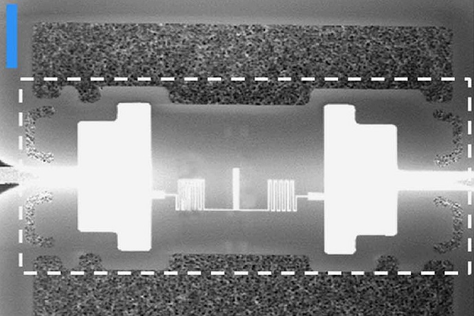
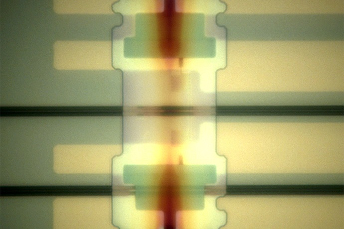
One of the researchers' devices during its transfer to an optical chip. Gold electrodes are deposited on a silicon nitride film at either end of a niobium nitride light detector.
Image courtesy of Nature Communications
Relocation
The researchers’ process begins with a silicon optical chip made using conventional manufacturing techniques. On a separate silicon chip, they grow a thin, flexible film of silicon nitride, upon which they deposit the superconductor niobium nitride in a pattern useful for photon detection. At both ends of the resulting detector, they deposit gold electrodes.
Then, to one end of the silicon nitride film, they attach a small droplet of polydimethylsiloxane, a type of silicone. They then press a tungsten probe, typically used to measure voltages in experimental chips, against the silicone.
“It’s almost like Silly Putty,” Englund says. “You put it down, it spreads out and makes high surface-contact area, and when you pick it up quickly, it will maintain that large surface area. And then it relaxes back so that it comes back to one point. It’s like if you try to pick up a coin with your finger. You press on it and pick it up quickly, and shortly after, it will fall off.”
With the tungsten probe, the researchers peel the film off its substrate and attach it to the optical chip.
In previous arrays, the detectors registered only 0.2 percent of the single photons directed at them. Even on-chip detectors deposited individually have historically topped out at about 2 percent. But the detectors on the researchers’ new chip got as high as 20 percent. That’s still a long way from the 90 percent or more required for a practical quantum circuit, but it’s a big step in the right direction.
“This work is a technical tour de force,” says Robert Hadfield, a professor of photonics at the University of Glasgow who was not involved in the research. “There is potential for scale-up to large circuits requiring hundreds of detectors using commercial pick-and-place technology.”

