Matthew Chin | February 02, 2015
A breakthrough by a team of researchers from UCLA, Columbia University and other institutions could lead to the more precise transfer of information in computer chips, as well as new types of optical materials for light emission and lasers.
The researchers were able to control light at tiny lengths around 500 nanometers — smaller than the light’s own wavelength — by using random crystal lattice structures to counteract light diffraction. The discovery could begin a new phase in laser collimation — the science of keeping lasers precise and narrow instead of spreading out.
The study’s principal investigator was Chee Wei Wong, associate professor of electrical engineering at the UCLA Henry Samueli School of Engineering and Applied Science.
Think of shining a flashlight against a wall. As the light moves from the flashlight and approaches the wall, it spreads out, a phenomenon called diffraction. The farther away the light source is held from the wall, the more the beam diffracts before it reaches the wall.
The same phenomenon also happens on a scale so small that distances are measured in nanometers — a unit equal to one-billionth of a meter. For example, light could be used to carry information in computer chips and optical fibers. But when diffraction occurs, the transfer of data isn’t as clean or precise as it could be.
Technology that prevents diffraction and more precisely controls the light used to transfer data could therefore lead to advances in optical communications, which would enable optical signal processing to overcome physical limitations in current electronics and could enable engineers to create improved optical fibers for use in biomedicine.
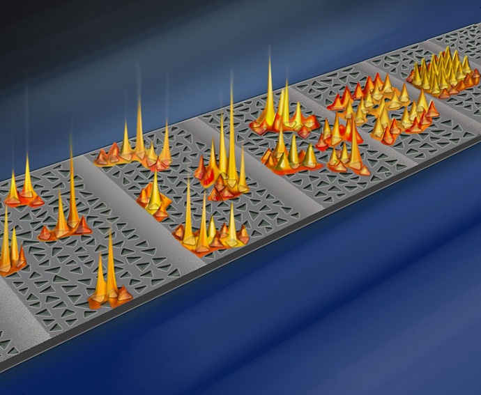
To control light on the nanoscale, the researchers used a photonic crystal superlattice, a lattice structure made of crystals that allows light through. The lattice was a disorderly pattern, with thousands of nanoscale heptagonal, square and triangular holes. These holes, each smaller than the wavelength of the light traveling through the structure, serve as guideposts for a beam of light.
Engineers had understood previously that uniformly patterned holes can control the spatial diffraction somewhat. But the researchers found in the new study that the structures with the most disorderly patterns were best able to trap and collimate the beam into a narrow path, and that the structure worked over a broad part of the infrared spectrum.
The study’s lead author was Pin-Chun Hsieh, who was advised by Wong during his doctoral studies at Columbia University’s Fu Foundation School of Engineering and Applied Science.
The effect of disorder, known as Anderson localization, was first proposed in 1958 by Nobel laureate Philip Anderson. It is the physical phenomenon that explains the conductance of electrons and waves in condensed matter physics.
The new study was the first to examine transverse Anderson localization in a chip-scale photonic crystal media. It was published online today by Nature Physics.
“This study allows us to validate the theory of Anderson localization in chip-scale photonics, through engineered randomness in an otherwise periodic structure,” Wong said. “What Pin-Chun has observed provides a new path in controlling light propagation at the wavelength scale, that is, delivering structure arising out of randomness.”
Hsieh, who also is chairman and majority owner of Taiwan-based Quantumstone Research, said the findings are completely counterintuitive because one might think that disorder in the structures would lead the light to spread out more. “This effect, based on intuition gained from electronic systems, where introduced impurities can turn an insulator into a semiconductor, shows unequivocally that controlling disorder can arrest transverse transport, and really reduce the spreading of light.”
The numerical simulation was performed at University College London, and the sample fabrication was carried out at the Brookhaven National Laboratory in New York and at National Cheng Kung University in Taiwan.
The research was supported primarily by a grant from the U.S. Office of Naval Research. Additional support was provided by the National Science Foundation, the Department of Energy and the government of the United Kingdom. Hsieh is supported by a scholarship from Taiwan’s Department of Education.

