2015.04.02
Researchers in the Sungkyunkwan University (SKKU) were able to develop a new doping technique for 2D nano-semiconductor using only heat and light energy. Doping is a process of altering the characteristics of a semiconductor by adjusting the concentration of the electrons or holes into n type or p type.
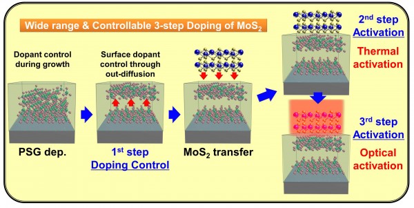
Prof. Park Jin-hong of SKKU Electrical and Computer Engineering and his team, used a silicate on top with a thin molybdenum disulfide (MoS2) nano-semiconductor to experiment with heat and light energy in the process.
As a result, the experiment on controlling the concentration of the holes was successful. This is the equivalent of 100 times the range area that can be conducted by conventional doping techniques.
“ I am certain that through this new doping technique, untilizing light and heat energy, we will be able to contribute to the progress of 2D nano-semicondutors” Prof. Park asserted.


