08/31/2015
Caltech engineers have created flat devices capable of manipulating light in ways that are very difficult or impossible to achieve with conventional optical components.
The new devices are not made of glass, but rather of silicon nanopillars that are precisely arranged into a honeycomb pattern to create a "metasurface" that can control the paths and properties of passing light waves.
These metasurface devices, described in a paper published online on August 31, 2015, in the journal Nature Nanotechnology, could lead to ultracompact optical systems such as advanced microscopes, displays, sensors, and cameras that can be mass-produced using the same photolithography techniques used to manufacture computer microchips.
"Currently, optical systems are made one component at a time, and the components are often manually assembled," says Andrei Faraon (BS '04), an assistant professor of applied physics and materials science, and the study's principal investigator. "But this new technology is very similar to the one used to print semiconductor chips onto silicon wafers, so you could conceivably manufacture millions of systems such as microscopes or cameras at a time."
Seen under a scanning electron microscope, the new metasurfaces that the team created resemble a cut forest where only the stumps remain. Each silicon stump, or pillar, has an elliptical cross section, and by carefully varying the diameters of each pillar and rotating them around their axes, the scientists were able to simultaneously manipulate the phase and polarization of passing light. Light is an electromagnetic field, and the field of single-color, or monochromatic, light oscillates at all points in space with the same frequency but varying relative delays, or phases.
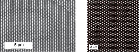
Scanning electron microscope of a metasurface showing silicon nano-pillars on a glass substrate. Tilted view is shown on the right and top view on the left. A honeycomb pattern is overlaid on the left image.
Credit: Dr. Amir Arbabi/Faraon Lab/Caltech
Manipulating this relative delay, or phase, influences the degree to which a light ray bends, which in turn influences whether an image is in or out of focus.
Polarization refers to the trajectory of the oscillations of the electromagnetic field at each point in space. Manipulating the polarization of light is essential for the operation of advanced microscopes, cameras, and displays; the control of polarization also enables simple gadgets such as 3-D glasses and polarized sunglasses.
"Using our metasurfaces, we have complete control of the polarization and phase of light," says study first author Amir Arbabi, a senior researcher at Caltech. "We can take any incoming light and shape its phase and polarization profiles arbitrarily and with very high efficiency."
While the same goal can be achieved using an arrangement of multiple conventional optical components such as glass lenses, prisms, spatial light modulators, polarizers, and wave plates, these many components lead to much bulkier systems. "If you think of a modern microscope, it has multiple components that have to be carefully assembled inside," Faraon says. "But with our platform, we can actually make each of these optical components and stack them atop one another very easily using an automated process. Each component is just a millionth of a meter thick, or less than a hundredth of the thickness of a human hair. "
In addition to being compact, a metasurface device could manipulate light in novel ways that are very hard and sometimes impossible to do using current setups. For example, the Caltech team showed that one of their metasurfaces can project one image when illuminated by a horizontally polarized beam of light, and a different image when illuminated by a vertically polarized beam. "The two images will appear overlapped under illumination with light polarized at 45 degrees," Faraon says.
In another experiment, the team was able to use a metasurface to create a beam with radial polarization, that is, a beam whose polarization is pointing toward the beam axis. Such beams have doughnut-shaped intensity profiles and have applications in superresolution microscopy, laser cutting, and particle acceleration. "You generally would need a large optical setup, consisting of multiple components, to create this effect using conventional instruments," Arbabi says. "With our setup, we can compress all of the optical components into one device and generate these beams with higher efficiency and more purity."
The team is currently working with industrial partners to create metasurfaces for use in commercial devices such as miniature cameras and spectrometers, but a limited number have already been produced for use in optical experiments by collaborating scientists in other disciplines.
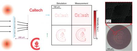
Projection of two different patterns by a single metasurface. Simulation and measurement results are shown in the middle, and optical and scanning electron images of the metasurface are shown on the left.
Credit: In press, Nature Nanotechnology
In addition, the Faraon lab current is investigating ways to combine different metasurfaces to create functioning optical systems and to correct for color distortions and other optical aberrations. "Like any optical system, you get distortions," Faraon said. "That's why expensive cameras have multiple lenses inside. Right now, we are experimenting with stacking different metasurfaces to correct for these aberrations and achieve novel functionalities."
The paper is entitled "Dielectric metasurfaces for complete control of phase and polarization with subwavelength spatial resolution and high transmission." In addition to Faraon and Arbabi, other Caltech coauthors include graduate student Yu Horie and Mahmood Bagheri, a microdevices engineer at JPL. The work was supported by the Caltech/JPL President's and Director's Fund and the Defense Advanced Research Projects Agency. Yu Horie was supported by the Department of Energy's Energy Frontier Research Center program and a Japan Student Services Organization fellowship. The device nanofabrication was performed in the Kavli Nanoscience Institute at Caltech.
Written by Ker Than

