April 04, 2014
As the properties and applications of graphene continue to be explored in laboratories all over the world, a growing number of researchers are looking beyond the one-atom-thick layer of carbon for alternative materials that exhibit similarly captivating properties.
One of these materials is molybdenum disulfide (MoS2), which is part of a wider group of materials known as transition metal dichalcogenides, and has been put forward by a group of researchers in the US as a potential building block for the next generation of low-cost electrical devices.
Due to its impressive ability to convert light into electricity at an extremely efficient rate, single layers of the semiconducting material have been used to fabricate a widely used device known as a photosensor, which is found in a range of appliances from solar panels and digital cameras to remote controls.
The device has been presented today, 4 April, in the very first issue of IOP Publishing’s new journal 2D Materials—a multidisciplinary journal with a focus on applications and fundamental science concerning all aspects of graphene and 2D materials.
In their study, the researchers highlighted the suitability of MoS2 by successfully demonstrating the photosensor’s ability to efficiently convert the energy from photons, delivered to the device in two separate wavelengths by a laser, into an electric current.
Lead author of the research, Nestor Perea-Lopez, from The Pennsylvania State University, said: “The thinnest foil of MoS2 has a thickness of three atoms. One can picture this monolayer foil as a sandwich, where sulfur atoms are the bread and molybdenum is the ham. The monolayer is even more interesting than the material in bulk, because in such thin form it can convert photons into electrons very efficiently, making it an ideal material to use in light detectors, such as the ones used in digital cameras.”
A significant challenge that remains for researchers working with 2D materials is how to produce the materials in bulk. Graphene, for example, can only be produced in bulk through a liquid phase or by exfoliating graphite into very thin layers or flakes, which can be very difficult to control.
The goal is to be able to synthesize 2D materials using a bottom-up approach, carefully piecing individual components together like building blocks.
The researchers did this successfully in their study by growing tiny triangles of single-layered MoS2, around five micrometers wide, onto a silica-based substrate using a bottom-up process known as chemical vapour deposition.
“The devices we built are very small which means that we could integrate millions in a few millimeter squares,” said Perea-Lopez.
On the suitability of MoS2 as an alternative to graphene, Perea-Lopez continued: “Graphene is a semi-metal, which means that electrons can move through the material very fast even with very small voltages; however, this is both an advantage and disadvantage, since electronic devices need to have an ‘on’ and ‘off’ state. Graphene devices can therefore be hard to turn off, but MoS2 has a large energy gap that allows it to have very large on/off ratios of hundreds of millions.
“Not everything about graphene is wrong though, and the path in this field must be the integration of metals and semi-metals, such as graphene, with insulators such as boron nitride and semiconductors like MoS2 to create the next generation of devices.”
The paper can be downloaded from http://iopscience.iop.org/2053-1583/1/1/011004/article

Researchers probe the next generation of 2D material
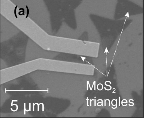
SEM micrograph showing the CVD-grown MoS2 triangular monolayers and the Au/Ti electrodes deposited on them by a combination of e-beam lithography and e-beam evaporation.

