April 10, 2014
For nearly a century, electrophoretic deposition (EPD) has been used as a method of coating material by depositing particles of various substances onto the surfaces of various manufactured items. One of the most common and oldest processes that utilize EPD is the application of a primer coat to new car bodies on a production assembly line. The body of the car is positively charged while the liquid primer in the dunk tank is negatively charged, forcing the attraction of the primer to the metal surface.
Since its earliest use, EPD has been used to deposit a wide range of materials on to surfaces, including ceramics, metals, polymers and even living cells. This tried and true process works well but it is limited. EPD can only deposit material across the entire surface and not in specific, predetermined locations, until now.
Scientists at Lawrence Livermore National Laboratory have created a technique called light-directed electrophoretic deposition, which uses photoconductive electrodes and DC electrical fields to dynamically pattern the surface material. This allows the buildup of material in targeted areas where the light comes in contact with the photoconductor’s surface. This enables the creation of arbitrarily patterned 3D multimaterial composites over large areas with fine resolution.
The research is the subject of a paper, “Light-Directed Electrophoretic Deposition: A New Additive Manufacturing Technique for Arbitrarily Patterned 3D Composites,” published in Advanced Materials.
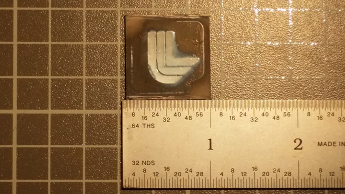
Researchers used light-directed EPD to produce an alumina ceramic- tungsten nanoparticle composite. Initially, the tungsten nanoparticles were deposited across the photoconductive surface, then illuminated through a laser cut aluminum mask. A different shaped mask was then substituted along with the new material, to deposit the ceramic material. In the future, the aluminum masks will be replaced by a digitally projected mask, similar to those found in DLP televisions, for a completely automated deposition system.
Light-directed electrophoretic deposition has the potential to elevate traditional EPD from a single layer, single material coating process to a true additive manufacturing technique that allows for unique composites to be formed. For example, void areas can be precisely created in a part to control polymer material behaviors for energy absorption or within cellular material for the creation of veins or blood vessels for manufactured organs.
“We have presented a novel electrophoretic deposition technique based on using light to pattern materials on a photoconductive layer. This represents a large step in advancing electrophoretic deposition as a method of fabricating complex 3D patterned composites”, said Andrew Pascall, research engineer and lead author.
More Information
"Light-Directed Electrophoretic Deposition: A New Additive Manufacturing Technique for Arbitrarily Patterned 3D Composites," Advanced Materials, April 9, 2014.

