May 22, 2014
In response to requests from the semiconductor industry,* a team of PML researchers has demonstrated that atomic force microscope (AFM) probe tips made from its near-perfect gallium nitride nanowires are superior in many respects to standard silicon or platinum tips in measurements of critical importance to microchip fabrication, nanobiotechnology, and other endeavors.
In addition, the scientists have invented a means of simultaneously using the nanowire tips as LEDs to illuminate a tiny sample region with optical radiation while it is scanning, adding an entirely new dimension to the characterization of nanoelectronics materials and devices.
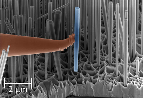
By itself, an AFM provides topographical information at nanometer resolution as its probe tip – in the range of 100 nm wide and suspended from a cantilever arm – scans across a sample surface. When the tip is used at the same time to continuously transmit and receive a microwave signal, the system becomes capable of revealing charge-carrier concentrations or defect locations in specific regions of nanoscale materials and devices.
That technique, called near-field scanning microwave microscopy (NSMM), had never before been attempted using a nanowire probe. But as the team showed in a recent paper in Applied Physics Letters, nanowire probe tips substantially outperformed commercial Pt tips in both resolution and durability.
“A big issue for platinum probes,” says Kris Bertness, Project Leader for Metrology and Synthesis of 3D Nanostructures in the Quantum Electronics and Photonics Division, “is that if you deform them even a little bit, and their shape changes, your calibration is lost. Because they’re capacitively coupled to the sample, shape is everything.
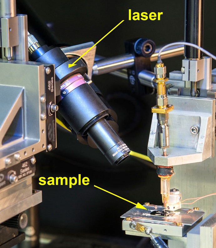
Illuminating an NSMM sample with a conventional laser brings light in at an angle and greatly increases the space occupied by apparatus.
“By contrast, our nanowire probe tips have a calibration lifetime about 10 times longer than any commercial tip. We see no visible wear after performing tens of scans, whereas platinum deforms, losing resolution and calibration, after five to ten scans.” In a series of 12 scans, the Pt tip radius changed from ~ 50 nm to ~150 nm. The nanowire, however, retained its original dimensions. Moreover, the GaN tips exhibited improved sensitivity and reduced uncertainty compared to a commercial Pt tip.
NSMM can produce very detailed imaging of the local density of positive and negative charge carriers inside a nanostructure – information of great practical significance to microdevice fabricators – and scientists from PML’s Electromagnetics Division have made notable progress in the technique. They believe that the use of nanowire probes, in conjunction with the recent arrival of a brand-new, custom-built, four-probe NSMM instrument, will reveal new aspects of nanostructure composition and performance. In biological materials, it could locate the attachment of chemical agents or particles that are bound to a cell, and aid in the study of protein dynamics.
Deploying a nanowire as a probe tip sounds deceptively simple. The researchers obtain a conventional AFM cantilever and probe, remove the existing tip, and use a device called a focused ion beam to drill a hole about 5 micrometers deep in the tip mount. Then, using a minuscule manipulator, they break off a single nanowire from a “forest” of them grown by molecular beam epitaxy, insert the wire into the hole, and weld it in place. Finally, the wire is coated with thin layers of titanium (20 nm) and aluminum (200 nm) in order to conduct the microwave signal all the way to the end of the tip and back.
The researchers tested their tip against a silicon tip, a platinum tip, and an uncoated GaN nanowire, each of which was scanned across an array of microcapacitors of different sizes. The coated nanowire proved about twice as sensitive as the Pt probe, and four times as sensitive as the others, with superior mechanical performance. “That can be extremely important for characterizing the next generation of advanced electronic and optoelectronic devices,” Bertness says. At present only a few GaN probes can be made at once, but the team is at work on developing ideas for producing them in wafer-scale quantities.
At the same time, the researchers are preparing to test a new technology for which they were awarded a patent in July, 2013: Using the nanowire tip as a light source by doping it so that it functions as an LED. Optical radiation can serve to excite the sample in a different way from the microwave signal, and scientists are already using lasers to illuminate nanoscale samples during AFM scans.
“The problem with that approach,” says veteran NSMM researcher Pavel Kabos of the Advanced High-Frequency Devices Program in PML’s Electromagnetics Division, “is that the laser has to shine in from the side. As a result, you get cast shadows and significant uncertainty as to exactly what area is being illuminated. And, of course, the laser and its mounting take up a great deal of space.
“With the new design, the illumination will be applied directly over the probe tip at the same place on the sample that is being exposed to the microwave signal. That could be particularly beneficial in characterizing photovoltaic materials where you could apply a light and get the carrier concentration at the same time. The whole unit can be much smaller, and the nanoscale light source enables you to inject some carriers very locally, in a way you can’t do with other methods.”In order to research the next generation of photovoltaic materials, Bertness says, “we’ve been using flood illumination. But what we want to see is how individual grains respond to light. The LED technique can make that possible. In biological applications, we expect it to provide an order of magnitude improvement in the ability to investigate processes such as protein dynamics.”
Reaching that goal will require more research into how to dope the GaN nanowires so as to increase efficiency of light output, and how to coordinate and integrate measurements from topographic, microwave, and optical modalities.
But Bertness is optimistic. “It took ten years of hard work learning how to fabricate and characterize these materials, and we developed a lot of important metrology techniques along the way. But we really weren’t able to test nanowires as probe tips until a few months ago when the Boulder lab’s Precision Imaging Facility gained a focused ion beam. These initial results give us confidence that this technology will impact a broad range of science and technology problems where knowing the properties of materials on the micrometer and nanometer scale is crucial, from semiconductor electronics to biochemistry and medicine.”
* The International Technology Roadmap for Semiconductors (ITRS), a periodic assessment of the semiconductor industry’s future technology requirements, has repeatedly called for progress in this area.
The 2011 ITRS said: “There is a need for characterizing the structure and local properties of current CMOS devices as they scale down… Recent developments in Scanning Probe Microscopy involving frequency-dependent signals on the sample and tip, and simultaneous perturbation with more than one frequency and/or probe expand the range and resolution of the measurements.”
The 2013 edition said: "Commercial vendors have developed a large toolbox of specialized SPM cantilevers and tips. Reproducibility is often an issue; in some cases yields of good tips are on the order of 30%. More important is the gap between commercially available cantilevers/tips and those required for tool development. … The lack of calibration standards for nm sized physical structures is a significant problem.”

