September 27, 2013
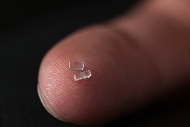
Menlo Park, Calif. — In an advance that could dramatically shrink particle accelerators for science and medicine, researchers used a laser to accelerate electrons at a rate 10 times higher than conventional technology in a nanostructured glass chip smaller than a grain of rice.
The achievement was reported today in Nature by a team including scientists from the U.S. Department of Energy’s (DOE) SLAC National Accelerator Laboratory and Stanford University.
“We still have a number of challenges before this technology becomes practical for real-world use, but eventually it would substantially reduce the size and cost of future high-energy particle colliders for exploring the world of fundamental particles and forces,” said Joel England, the SLAC physicist who led the experiments. “It could also help enable compact accelerators and X-ray devices for security scanning, medical therapy and imaging, and research in biology and materials science.”
Because it employs commercial lasers and low-cost, mass-production techniques, the researchers believe it will set the stage for new generations of "tabletop" accelerators.
At its full potential, the new “accelerator on a chip” could match the accelerating power of SLAC’s 2-mile-long linear accelerator in just 100 feet, and deliver a million more electron pulses per second.
This initial demonstration achieved an acceleration gradient, or amount of energy gained per length, of 300 million electronvolts per meter. That's roughly 10 times the acceleration provided by the current SLAC linear accelerator.
“Our ultimate goal for this structure is 1 billion electronvolts per meter, and we’re already one-third of the way in our first experiment,” said Stanford Professor Robert Byer, the principal investigator for this research.
Today’s accelerators use microwaves to boost the energy of electrons. Researchers have been looking for more economical alternatives, and this new technique, which uses ultrafast lasers to drive the accelerator, is a leading candidate.
Particles are generally accelerated in two stages. First they are boosted to nearly the speed of light. Then any additional acceleration increases their energy, but not their speed; this is the challenging part.
In the accelerator-on-a-chip experiments, electrons are first accelerated to near light-speed in a conventional accelerator. Then they are focused into a tiny, half-micron-high channel within a fused silica glass chip just half a millimeter long. The channel had been patterned with precisely spaced nanoscale ridges. Infrared laser light shining on the pattern generates electrical fields that interact with the electrons in the channel to boost their energy. (See the accompanying animation for more detail.)
Turning the accelerator on a chip into a full-fledged tabletop accelerator will require a more compact way to get the electrons up to speed before they enter the device.
A collaborating research group in Germany, led by Peter Hommelhoff at Friedrich Alexander University and the Max Planck Institute of Quantum Optics, has been looking for such a solution. It simultaneously reports in Physical Review Letters its success in using a laser to accelerate lower-energy electrons.
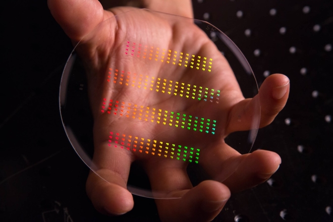
The nanoscale patterns of SLAC and Stanford's accelerator on a chip gleam in rainbow colors prior to being assembled and cut into their final forms. (Matt Beardsley/SLAC)
Applications for these new particle accelerators would go well beyond particle physics research. Byer said laser accelerators could drive compact X-ray free-electron lasers, comparable to SLAC’s Linac Coherent Light Source, that are all-purpose tools for a wide range of research.
Another possible application is small, portable X-ray sources to improve medical care for people injured in combat, as well as provide more affordable medical imaging for hospitals and laboratories. That’s one of the goals of the Defense Advanced Research Projects Agency’s (DARPA) Advanced X-Ray Integrated Sources (AXiS) program, which partially funded this research. Primary funding for this research is from the DOE’s Office of Science. 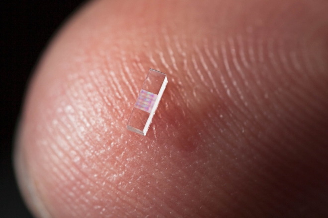
The key to the accelerator chips is tiny, precisely spaced ridges, which cause the iridescence seen in this close-up photo. (Matt Beardsley/SLAC)
The study's lead authors were Stanford graduate students Edgar Peralta and Ken Soong. Peralta created the patterned fused silica chips in the Stanford Nanofabrication Facility. Soong implemented the high-precision laser optics for the experiment at SLAC’s Next Linear Collider Test Accelerator. Additional contributors included researchers from the University of California-Los Angeles and Tech-X Corp. in Boulder, Colo.
Citation: E. A. Peralta et al., Nature, 27 Sept 2013 (10.1038/nature12664)

