May 16, 2013
David L. Chandler, MIT News Office
Graphene has dazzled scientists, ever since its discovery more than a decade ago, with its unequalled electronic properties, its strength and its light weight. But one long-sought goal has proved elusive: how to engineer into graphene a property called a band gap, which would be necessary to use the material to make transistors and other electronic devices.
Now, new findings by researchers at MIT are a major step toward making graphene with this coveted property. The work could also lead to revisions in some theoretical predictions in graphene physics.
The new technique involves placing a sheet of graphene — a carbon-based material whose structure is just one atom thick — on top of hexagonal boron nitride, another one-atom-thick material with similar properties. The resulting material shares graphene’s amazing ability to conduct electrons, while adding the band gap necessary to form transistors and other semiconductor devices.
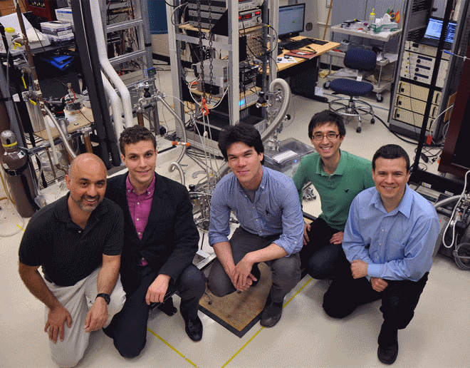
The work is described in a paper in the journal Science co-authored by Pablo Jarillo-Herrero, the Mitsui Career Development Assistant Professor of Physics at MIT, Professor of Physics Ray Ashoori, and 10 others.
“By combining two materials,” Jarillo-Herrero says, “we created a hybrid material that has different properties than either of the two.”
Graphene is an extremely good conductor of electrons, while boron nitride is a good insulator, blocking the passage of electrons. “We made a high-quality semiconductor by putting them together,” Jarillo-Herrero explains. Semiconductors, which can switch between conducting and insulating states, are the basis for all modern electronics.
To make the hybrid material work, the researchers had to align, with near perfection, the atomic lattices of the two materials, which both consist of a series of hexagons. The size of the hexagons (known as the lattice constant) in the two materials is almost the same, but not quite: Those in boron nitride are 1.8 percent larger. So while it is possible to line the hexagons up almost perfectly in one place, over a larger area the pattern goes in and out of register.
At this point, the researchers say they must rely on chance to get the angular alignment for the desired electronic properties in the resulting stack. However, the alignment turns out to be correct about one time out of 15, they say.
“The qualities of the boron nitride bleed over into the graphene,” Ashoori says. But what’s most “spectacular,” he adds, is that the properties of the resulting semiconductor can be “tuned” by just slightly rotating one sheet relative to the other, allowing for a spectrum of materials with varied electronic characteristics.
Others have made graphene into a semiconductor by etching the sheets into narrow ribbons, Ashoori says, but such an approach substantially degrades graphene’s electrical properties. By contrast, the new method appears to produce no such degradation.
The band gap created so far in the material is smaller than that needed for practical electronic devices; finding ways of increasing it will require further work, the researchers say.
“If … a large band gap could be engineered, it could have applications in all of digital electronics,” Jarillo-Herrero says. But even at its present level, he adds, this approach could be applied to some optoelectronic applications, such as photodetectors.
The results “surprised us pleasantly,” Ashoori says, and will require some explanation by theorists. Because of the difference in lattice constants of the two materials, the researchers had predicted that the hybrid’s properties would vary from place to place. Instead, they found a constant, and unexpectedly large, band gap across the whole surface.
In addition, Jarillo-Herrero says, the magnitude of the change in electrical properties produced by putting the two materials together “is much larger than theory predicts.”
The MIT team also observed an interesting new physical phenomenon. When exposed to a magnetic field, the material exhibits fractal properties — known as a Hofstadter butterfly energy spectrum — that were described decades ago by theorists, but thought impossible in the real world. There is intense research in this area; two other research groups also report on these Hofstadter butterfly effects this week in the journal Nature.
Eva Andrei, a professor of physics at Rutgers University who was not involved in this work, says that until recently, “decades-old theoretical predictions of novel and surprising physical phenomena, expected to occur in 2-D electron systems [such as graphene], have lain dormant.” But the MIT team’s work clearly demonstrates some of these phenomena, she says.
“Perhaps most significant is their observation of a band gap in zero magnetic field,” she says. “The ability to induce a zero-field band gap in graphene may one day allow its use as a switch in transistor applications, providing a viable and inexpensive alternative to silicon electronics.”
The research included postdocs Ben Hunt and Andrea Young and graduate student Javier Sanchez-Yamagishi, as well as six other researchers from the University of Arizona, the National Institute for Materials Science in Tsukuba, Japan, and Tohoku University in Japan. The work was funded by the U.S. Department of Energy, the Gordon and Betty Moore Foundation and the National Science Foundation.

