October 1, 2013
[PTB/es] Graphene, a crystal composed of only one layer of carbon atoms arranged in a regular hexagon, is regarded as a material which is believed to be capable of performing miracles, in particular in the fields of electronics, sensor technology and display technology, but also in metrology. Only four years after the first successful preparation of graphene, its discoverers Geim and Novoselov were therefore awarded a Nobel Prize. As the original preparation method (flaking of single atomic layers of graphite) does not offer a good perspective for broad technological use, many groups of researchers are concentrating very strongly on the development of alternative manufacturing procedures. A completely new and very flexible variant has now been developed by the group of Andrey Turchanin from the University of Bielefeld in cooperation with the University of Ulm and three departments of the Physikalisch-Technische Bundesanstalt (PTB) and this has been published in the scientific journal "Advanced Materials".
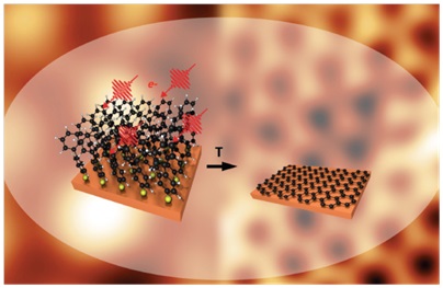
In contrast to the conventional methods where graphene is manufactured, for example, by precipitation of carbon atoms from the gas phase or by thermal graphitization of silicon carbide, the scientists selected aromatic molecules as a starting point in this work. As substrates, both copper single-crystals and inexpensive polycrystalline copper foils were used. By irradiation with low-energy electrons and subsequent thermal annealing, it was then possible to convert a self-organized single-layer of the molecule biphenyl thiol, which had precipitated on the copper surface, into graphene.
To investigate the chemical and physical properties of the graphene manufactured in this way, different characterization methods from Ulm and Bielefeld universities and from PTB were applied, for example, scanning tunnelling microscopy, transmission electron microscopy, Raman spectroscopy as well as electric transport measurements at low temperatures and high magnetic fields. All these measurements confirm that graphene of excellent crystalline and electronic quality had actually been manufactured from the aromatic molecule. The flexibility of the electron irradiation, which is possible both over large areas and also with excellent spatial resolution at small, well-defined places, now allows graphene structures of basically any form to be manufactured, e.g. quantum dots, nanoribbons or other nano-geometries with specific functionality. The selection of the temperature in the thermal conversion step also allows the degree of crystallinity and the characteristics of the graphene depending on it to be adjusted.
Additional advantages result from the versatility of the method of self-organized coating. It can be performed with different aromatic molecules which could, for example, also contain doping atoms for electronic doping of the final product. Applied in multiple layers, so-called bi-layer or multi-layer graphene could be manufactured, whose changed electronic band structure expands the potential applications of single-layer graphene. Likewise, other substrates than the copper used here (for example other metals, semiconductors, isolators) can be used. In addition, it should also be possible to manufacture graphene on any three-dimensional surfaces, as molecular self-organization also takes place on curved surfaces. The new manufacturing method broadens the perspectives for an improved use of the "magic material" in such an impressive way that the respective publication was emphasized on the cover sheet of the August issue of the scientific journal "Advanced Materials".
Original publication
D. G. Matei, N.-E. Weber, S. Kurasch, S. Wundrack, M. Woszczyna, M. Grothe, T. Weimann, F.-J. Ahlers, R. Stosch, U. Kaiser, A. Turchanin: Functional single-layer graphene sheets from aromatic monolayers. Advanced Materials, 25 (2013), 30, 4146-4151 , dx.doi.org/10.1002/adma.201300651 [article], dx.doi.org/10.1002/adma.201370195 [frontispiece]; Wiley-VCH. ISSN 1521-4095

