March 5, 2014
By Cory Nealon
BUFFALO, N.Y. – Associated with unhappy visits to the dentist, “cavity” means something else in the branch of physics known as optics.
Put simply, an optical cavity is an arrangement of mirrors that allows beams of light to circulate in closed paths. These cavities help us build things like lasers and optical fibers used for communications.
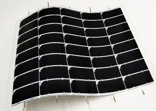
Now, an international research team pushed the concept further by developing an optical “nanocavity” that boosts the amount of light that ultrathin semiconductors absorb. The advancement could lead to, among other things, more powerful photovoltaic cells and faster video cameras; it also could be useful for splitting water using energy from light, which could aid in the development of hydrogen fuel.
The team, comprised of faculty and students from the University at Buffalo and two Chinese universities, presented its findings Feb. 24 in the journal Advanced Materials. The paper, called “Nanocavity enhancement for ultra-thin film optical absorber,” is available here: http://bit.ly/1bGGIbO.
“We’re just scratching the surface, but the preliminary work that we’ve done is very promising,” said Qiaoqiang Gan, PhD, lead author and UB assistant professor of electrical engineering. “This advancement could lead to major breakthroughs in energy-harvesting and conversion, security and other areas that will benefit humankind.”
Semiconductors form the basis of modern electronics. They work by manipulating the flow of energy in electronic devices. The most common semiconductor material, silicon, is used to make microchips for cellular phones, computers and other electronic devices.
Industry has kept pace with the demand for smaller, thinner and more powerful optoelectronic devices, in part, by shrinking the size of the semiconductors used in these devices.
The problem, however, is that these ultrathin semiconductors do not absorb light as well as conventional bulk semiconductors. Therefore, there is an intrinsic tradeoff between the ultrathin semiconductors’ optical absorption capacity and their ability to generate electricity.
As a result, researchers worldwide are trying to find ways to boost the amount of light that ultrathin semiconductors can absorb. Harvard University researchers recently had varying degrees of success by combining thin films of germanium, another common semiconductor, on a gold surface.
“While the results are impressive, gold is among the most expensive metals,” said Suhua Jiang, associate professor of materials science at Fudan University in China. “We illustrated a nanocavity, made with aluminum or other whitish metals and alloys that are far less expensive, can be used to increase the amount of light that semiconducting materials absorb.”
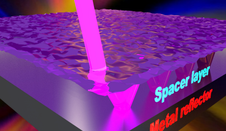
The nanocavity consists of, from bottom to top: aluminum, aluminum oxide and germanium. In the experiment, light passed through the germanium, which is 1.5 to 3 nanometers thick, and circulated in a closed path through the aluminum oxide and aluminum.
The absorption rate peaked at 90 percent, with germanium absorbing roughly 80 percent of the blue-green light and aluminum absorbing the rest. This is ideal, said Haomin Song, PhD candidate in electrical engineering at UB and the paper’s first author, because the bulk of the light stays within the semiconducting material.
“The nanocavity has many potential applications. For example, it could help boost the amount of light that solar cells are able to harvest; it could be implanted on camera sensors, such as those used for security purposes that require a high-speed response. It also has properties that could be useful for photocatalytic water splitting, which could help make hydrogen fuel a reality,” Song said.
Before any of that happens, however, more research must be done, especially as it relates to how the semiconductor would turn the light into power as opposed to heat.
Gan’s research group is collaborating with Alexander Cartwright, PhD, UB professor of electrical engineering and vice president for research and economic development, and Mark Swihart, PhD, UB professor of chemical and biological engineering, to develop ultrathin energy-harvesting devices.
Gan is also working with Hao Zeng, PhD, UB associate professor of physics, to study its effect on photocatalysis.
In addition to Gan, Jiang and Song, the paper’s other authors are: UB PhD candidates in electrical engineering Dengxin Ji, Kai Liu, Xie Zeng and Nan Zhang; Luqing Guo and Zhejun Liu, both PhD candidates at Fudan; and Haifeng Hu, assistant professor at Northeastern University in China.
The National Science Foundation supported the research.
Gan is a member of UB’s electrical engineering optics and photonics research group, which includes Cartwright, professors Edward Furlani and Pao-Lo Liu; associate professor Natalia Litchinitser; and assistant professor Liang Feng.
The group carries out research in nanophotonics, biophotonics, hybrid inorganic/organic materials and devices, nonlinear and fiber optics, metamaterials, nanoplasmonics, optofluidics, microelectromechanical systems (MEMS), biomedical microelectromechanical systems (BioMEMs), biosensing and quantum information processing.

