2020.06.23
South Korean researchers have succeeded in implementing a three-dimensional display with output characteristics that cannot be seen on flat-panel displays. GIST (Gwangju Institute of Science and Technology, President Kiseon Kim) School of Materials Science and Engineering Professor Heung Cho Ko's research team developed a display capable of output in various directions by transforming a flexible electrode-based flat panel display in three dimensions using origami.
Displays are a representative electronic device that mainly expresses electrically transmitted video signals in human recognizable form and is commonly used in TVs, mobile phones, monitors, electronic displays, black boxes, smartwatches, virtual reality machines, displays for vehicles, etc. Most of these displays have a flat structure depending on the manufacturing process.
Unlike conventional flat-panel displays that can only show images in one direction, the 3-D structure display can show images in various directions, allowing them to be applied to virtual reality/enhanced displays, head mounted displays, double-sided displays, building/vehicle interior and exterior displays, creating high-value next-generation technologies.
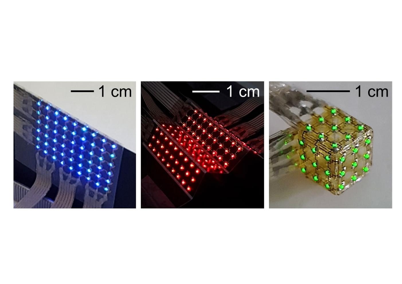
The research team produced and modified a flexible thin-film electrode-based display thinner than 10 micrometers (μm) for the development of a three dimensional display.
The research team made a thin film electrode on an acrylonitrile butadiene styrene (ABS) film, then transferred the LED to make a display, and injected the volatile solvent into a microfluidic channel* optionally plasticized** to the desired location.
Even if the plasticized polymer film was selectively folded inwards and outwards through plastic deformation***, it did not affect the characteristics of electronic devices, so it was possible to transform flat display devices into various forms using origami. The method of implementing a 3D electronic device through deformation after fabrication of a thin-film electronic device in such a plane has an advantage in that performance or resolution of the electronic device is not deteriorated, and most of the existing semiconductor processing equipment can be used.
Through this method, Professor Heung Cho Ko's research team succeeded in implementing a double-sided display capable of outputting images back and forth, a holographic display showing different images depending on the viewing angle, and a hexahedral display capable of outputting in all directions.
Professor Heung Cho Ko said, "The biggest significance of this study is to propose a technology that can be freely transformed into a three-dimensional structure while maintaining the ideal circuit structure that the device must have in the development of a three-dimensional electronic device through the transformation of flexible electronic devices. In the future, it will be utilized in the development of various 3D structure sensors along with displays, and will be used to develop input/output devices for broadcasting, medical, aviation, military, advertising, animation, and movies."
This study was conducted with the support of the Ministry of Science and ICT and the Korea Research Foundation as a basic research project (medium-sized researcher), and the results were selected as the cover paper for the June issue of Advanced Materials Technologies, an international journal for new materials, and was published on June 11, 2020.
* microfluidic channel: semiconductor process allows for spatial and temporal control of fluids through micro or nano-sized tubes
** plasticization: inject heat or solvents into a polymer so that it can be permanently deformed
*** plastic deformation: When an object is deformed by applying an external force, it retains the deformed shape without returning to its original state even after removing the external force.