21. January 2015
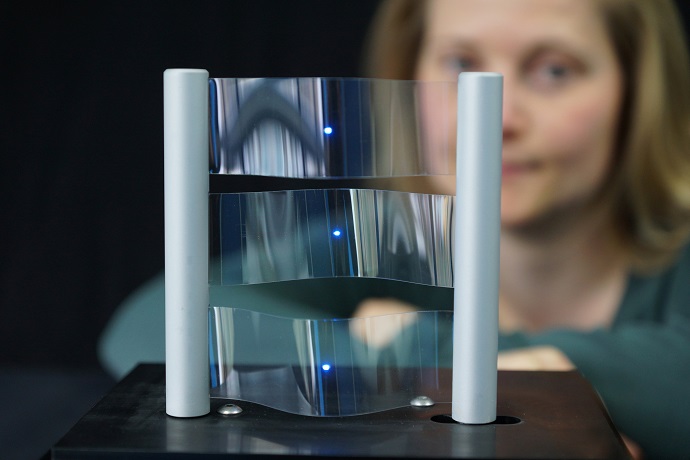
Mobile phones and smart phones still haven‘t been adapted to the carrying habits of their users. That much is clear to anyone who has tried sitting down with a mobile phone in their back pocket: the displays of the innumerable phones and pods are rigid and do not yield to the anatomical forms adopted by the people carrying them. By now it is no longer any secret that the big players in the industry are working on flexible displays. Properties that suitable coatings offer in this respect will be demonstrated by the developments of the INM – Leibniz-Institute for New Materials on show nano tech 2015, Tokio, Japan.
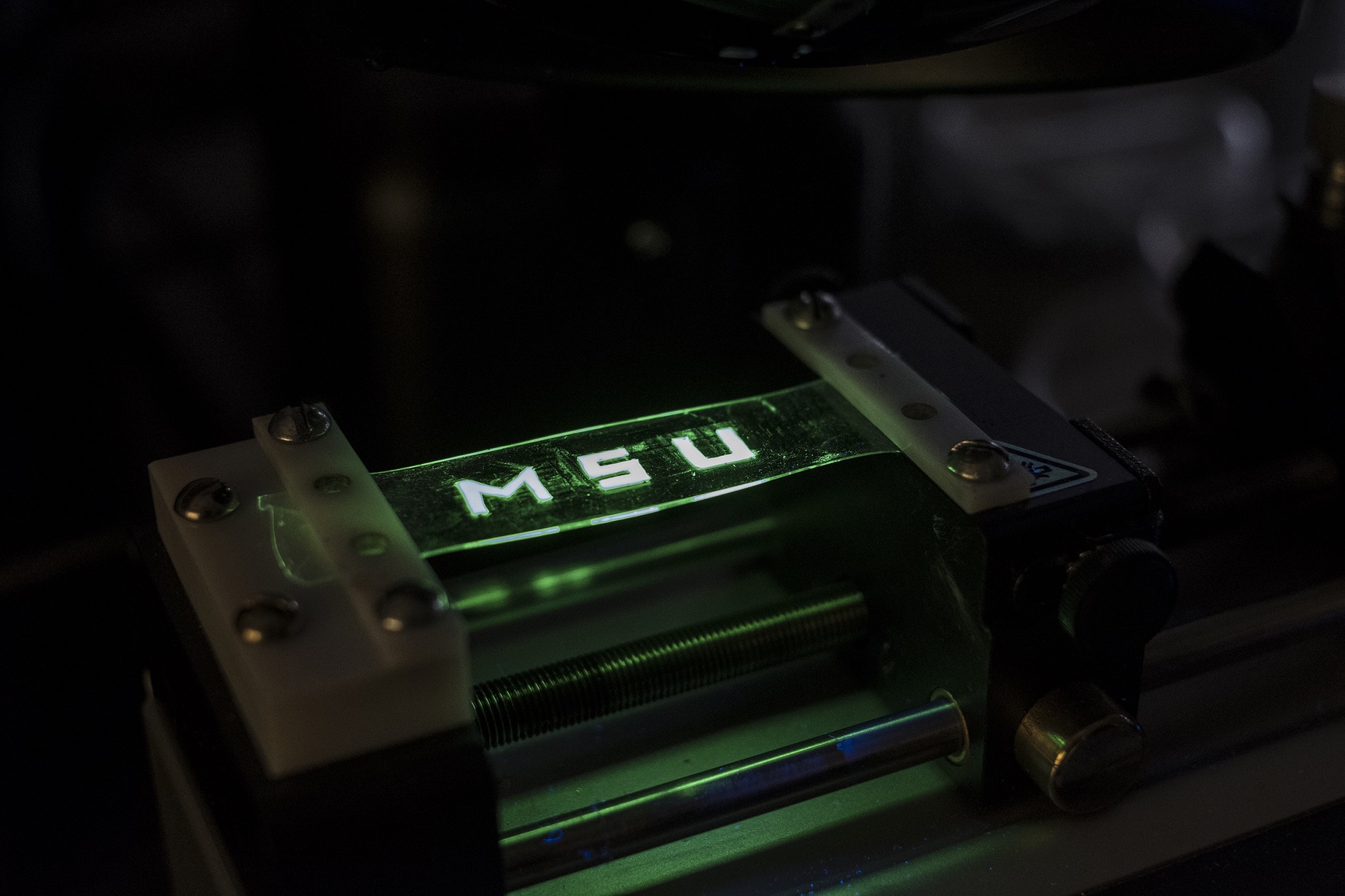
For the nanoparticle inks, the researchers are using what are known as TCOs, or transparent conducting oxides. “We use the TCOs to produce nanoparticles with special properties”, says Peter William de Oliveira, Head of the Optical Materials Program Division, “the TCO ink is then created by adding a solvent and a special binder to these TCO particles”. The binder performs several tasks here: it not only makes the TCO nanoparticles adhere well on the film; it also increases the flexibility of the TCO coating: in this way, the conductivity is maintained even when the films are bent. The ink can then be applied to the film directly by gravure printing using a printing plate. After curing under UV light at 150°C, the coating is ready.
The transparent electronic inks allow conductor tracks to be produced unproblematically even on a large-scale by means of the classic reel-to-reel process. Initial trials at INM have been promising. The researchers all agree that the use of structured rollers will in the future allow even large, structured conductive surfaces to be printed with a high throughput at low cost. Conductive coatings with TCOs are usually applied by means of high vacuum techniques. The method known as sputtering, however, is very expensive.
From January 28 to 30, the researchers of the INM will present this and further results at the German Pavilion, Booth 5J-21. At the German Pavilion, the Association of German Engineers (VDI) will concentrate the expertise of all German exhibitors at the nano tech. The German Pavilion is supported by the Federal Ministry for Economic Affairs and Energy (BMWi). An oral presentation on „Materials and Processing for functionalized Surfaces“. will take place at the Main Theater, Hall 5, on January 29, German Day.
INM conducts research and development to create new materials – for today, tomorrow and beyond. Chemists, physicists, biologists, materials scientists and engineers team up to focus on these essential questions: Which material properties are new, how can they be investigated and how can they be tailored for industrial applications in the future? Four research thrusts determine the current developments at INM: New materials for energy application, new concepts for medical surfaces, new surface materials for tribological applications and nano safety and nano bio. Research at INM is performed in three fields: Nanocomposite Technology, Interface Materials, and Bio Interfaces.
INM – Leibniz Institute for New Materials, situated in Saarbruecken, is an internationally leading centre for materials research. It is an institute of the Leibniz Association and has about 195 employees.