December 11, 2014
By Robert Sanders
BERKELEY —The entire semiconductor industry, not to mention Silicon Valley, is built on the propensity of electrons in silicon to get kicked out of their atomic shells and become free. These mobile electrons are routed and switched though transistors, carrying the digital information that characterizes our age.
An international team of physicists and chemists based at UC Berkeley has, for the first time, taken snapshots of this ephemeral event using attosecond pulses of soft X-ray light lasting only a few billionths of a billionth of a second.
While earlier femtosecond lasers were unable to resolve the jump from the valence shell of the silicon atom across the band-gap into the conduction electron region, the new experiments now show that this transition takes less than 450 attoseconds.
“Though this excitation step is too fast for traditional experiments, our novel technique allowed us to record individual snapshots that can be composed into a ‘movie’ revealing the timing sequence of the process,” explains Stephen Leone, UC Berkeley professor of chemistry and physics.
Leone, his UC Berkeley colleagues and collaborators from the Ludwig-Maximilians Universität in Munich, Germany, the University of Tsukuba, Japan, and the Molecular Foundry at the Department of Energy’s Lawrence Berkeley National Laboratory report their achievement in the Dec. 12 issue of the journal Science.
Century-old discovery observed
Leone notes that more than a century has elapsed since the discovery that light can make certain materials conductive. The first movie of this transition follows the excitation of electrons across the band-gap in silicon with the help of attosecond extreme ultraviolet (XUV) spectroscopy, developed in the Attosecond Physics Laboratory run by Leone and Daniel Neumark, UC Berkeley professor of chemistry.
In semiconducting materials, electrons are initially localized around the individual atoms forming the crystal and thus cannot move or contribute to electrical currents. When light hits these materials or a voltage is applied, some of the electrons absorb energy and get excited into mobile states in which the electrons can move through the material. The localized electrons take a “quantum jump” into the conduction band, tunneling through the barrier that normally keeps them bound to atoms.
These mobile electrons make the semiconductor material conductive so that an applied voltage results in a flowing current. This behavior allows engineers to make silicon switches, known as transistors, which have become the basis of all digital electronics.
The researchers used attosecond XUV spectroscopy like an attosecond stop watch to follow the electron’s transition. They exposed a silicon crystal to ultrashort flashes of visible light emitted by a laser source. The subsequent illumination with X-ray-pulses of only a few tens of attoseconds (10-18 seconds) in duration allowed the researchers to take snapshots of the evolution of the excitation process triggered by the laser pulses.
Unambiguous interpretation of the experimental data was facilitated by a series of supercomputer simulations carried out by researchers at the University of Tsukuba and the Molecular Foundry. The simulations modeled both the excitation process and the subsequent interaction of X-ray pulses with the silicon crystal.
Electron jump makes atoms rebound
The excitation of a semiconductor with light is traditionally conceived as a process involving two distinct events. First, the electrons absorb light and get excited. Afterwards, the lattice, composed of the individual atoms in the crystal, rearranges in response to this redistribution of electrons, turning part of the absorbed energy into heat carried by vibrational waves called phonons.
In analyzing their data, the team found clear indications that this hypothesis is true. They showed that initially, only the electrons react to the impinging light while the atomic lattice remains unaffected. Long after the excitation laser pulse has left the sample – some 60 femtoseconds later – they observed the onset of a collective movement of the atoms, that is, phonons. This is near the 64 femtosecond period of the fastest lattice vibrations.
![]()
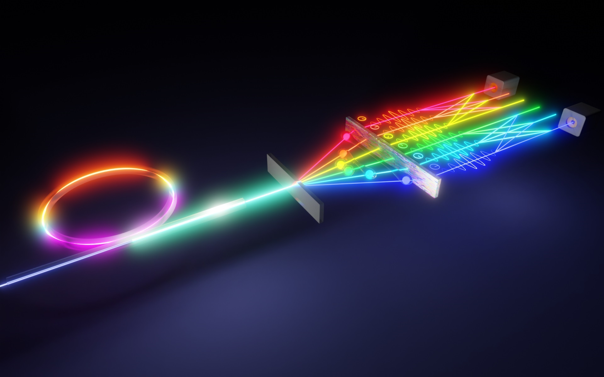
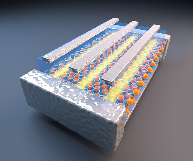
A series of snapshots of the electron energies in a silicon crystal. From back to front, the atom-bound electrons have a very narrow, sharply peaked range of energies (red), but once the electrons jump to the conduction band, the energy distribution spreads out (orange and yellow). The jump takes only 450 attoseconds. UC Berkeley image.
Based on current theory, the researchers calculated that the lattice spacing rebounded about 6 picometers (10-12meters) as a result of the electron jump, consistent with other estimates.
“These results represent a clean example of attosecond science applied to a complex and fundamentally important system,” Neumark says.
The unprecedented temporal resolution of this attosecond technology will allow scientists to resolve extremely brief electronic processes in solids that to date seemed too fast to be approached experimentally, says Martin Schultze, who was a guest researcher in Leone’s lab last year, visiting from the Ludwig-Maximilians Universität München. This poses new challenges to the theory of light-matter interactions, including the excitation step, its timescale and the interpretation of experimental X-ray spectra.
“But here is also an advantage,” Schultze adds. “With our ultrashort excitation and probing pulses, the atoms in the crystal can be considered frozen during the interaction. That eases the theoretical treatment a lot.”
Other co-authors are Krupa Ramasesha, D. Whitmore, A. Gandman, James S. Prell and L. J. Borja of UC Berkeley; C.D. Pemmaraju and D. Prendergast of the Molecular Foundry; and S.A. Sato and K. Yabana of Tsukuba.
The work was funded by the U.S. Department of Defense and the Defense Advanced Research Projects Agency’s PULSE program. Supercomputing resources were provided by Lawrence Berkeley National Laboratory, the National Energy Research Scientific Computing Center (NERSC) and the Institute of Solid State Physics, University of Tokyo.
RELATED INFORMATION
Attosecond band gap dynamics in Silicon (12/12/14 Science)
Attosecond Physics Laboratory


