April 16, 2014
David L. Chandler | MIT News Office
A quasiparticle called an exciton — responsible for the transfer of energy within devices such as solar cells, LEDs, and semiconductor circuits — has been understood theoretically for decades. But exciton movement within materials has never been directly observed.
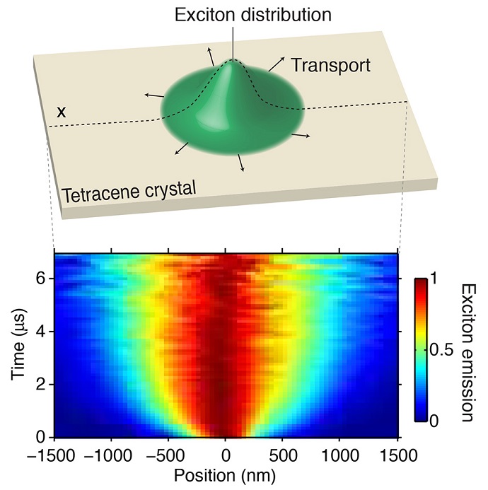
Now scientists at MIT and the City University of New York have achieved that feat, imaging excitons’ motions directly. This could enable research leading to significant advances in electronics, they say, as well as a better understanding of natural energy-transfer processes, such as photosynthesis.
The research is described this week in the journal Nature Communications, in a paper co-authored by MIT postdocs Gleb Akselrod and Parag Deotare, professors Vladimir Bulovic and Marc Baldo, and four others.
“This is the first direct observation of exciton diffusion processes,” Bulovic says, “showing that crystal structure can dramatically affect the diffusion process.”
“Excitons are at the heart of devices that are relevant to modern technology,” Akselrod explains: The particles determine how energy moves at the nanoscale. “The efficiency of devices such as photovoltaics and LEDs depends on how well excitons move within the material,” he adds.
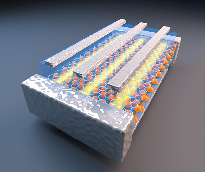
An exciton, which travels through matter as though it were a particle, pairs an electron, which carries a negative charge, with a place where an electron has been removed, known as a hole. Overall, it has a neutral charge, but it can carry energy. For example, in a solar cell, an incoming photon may strike an electron, kicking it to a higher energy level. That higher energy is propagated through the material as an exciton: The particles themselves don’t move, but the boosted energy gets passed along from one to another.
While it was previously possible to determine how fast, on average, excitons could move between two points, “we really didn’t have any information about how they got there,” Akselrod says. Such information is essential to understanding which aspects of a material’s structure — for example, the degree of molecular order or disorder — might facilitate or slow that motion.
“People always assumed certain behavior of the excitons,” Deotare says. Now, using this new technique — which combines optical microscopy with the use of particular organic compounds that make the energy of excitons visible — “we can directly say what kind of behavior the excitons were moving around with.” This advance provided the researchers with the ability to observe which of two possible kinds of “hopping” motion was actually taking place.
“This allows us to see new things,” Deotare says, making it possible to demonstrate that the nanoscale structure of a material determines how quickly excitons get trapped as they move through it.
For some applications, such as LEDs, Deotare says, it is desirable to maximize this trapping, so that energy is not lost to leakage; for other uses, such as solar cells, it is essential to minimize the trapping. The new technique should allow researchers to determine which factors are most important in increasing or decreasing this trapping.
“We showed how energy flow is impeded by disorder, which is the defining characteristic of most materials for low-cost solar cells and LEDs,” Baldo says.
While these experiments were carried out using a material called tetracene — a well-studied archetype of a molecular crystal — the researchers say that the method should be applicable to almost any crystalline or thin-film material. They expect it to be widely adopted by researchers in academia and industry.
“It’s a very simple technique, once people learn about it,” Akselrod says, “and the equipment required is not that expensive.”
Exciton diffusion is also a basic mechanism underlying photosynthesis: Plants absorb energy from photons, and this energy is transferred by excitons to areas where it can be stored in chemical form for later use in supporting the plant’s metabolism. The new method might provide an additional tool for studying some aspects of this process, the team says.
David Lidzey, a professor of physics and astronomy at the University of Sheffield who was not involved in this work, calls the research “a really impressive demonstration of a direct measurement of the diffusion of triplet excitons and their eventual trapping.” He adds, “Exciton diffusion and transport are important processes in solar-cell devices, so understanding what limits these may well help the design of better materials, or the development of better ways to process materials so that energy losses during exciton migration are limited.”
The work was supported by the U.S. Department of Energy and by the National Science Foundation, and used facilities of the Eni-MIT Solar Frontiers Center.

