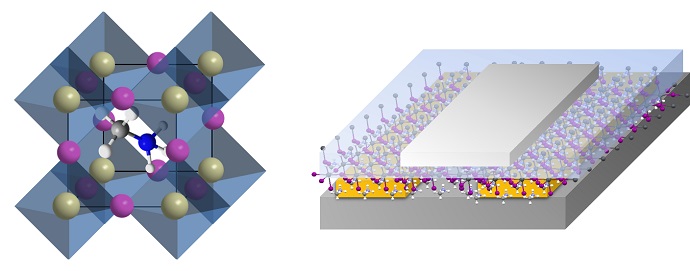
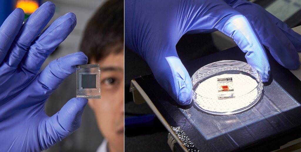
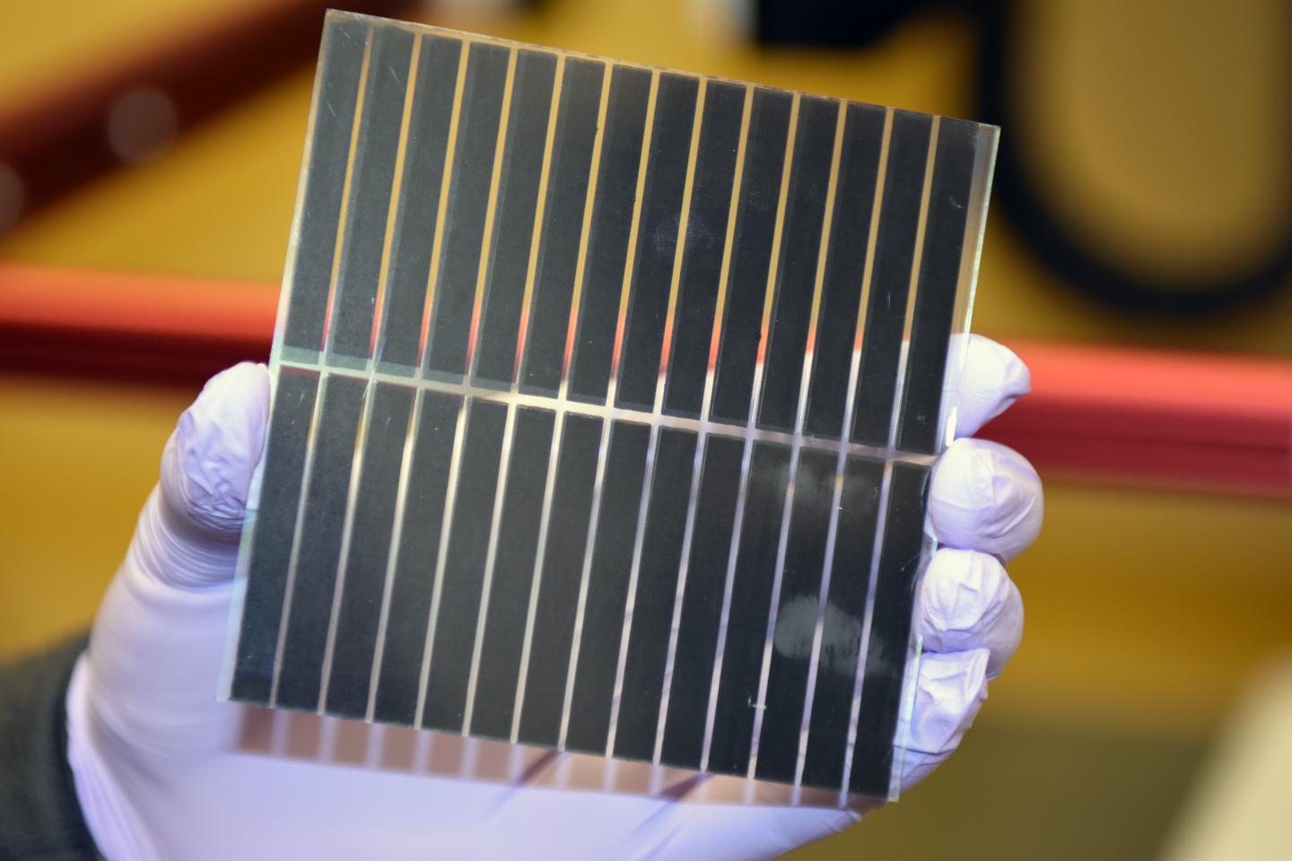
May 5, 2015 – Researchers from Wake Forest University and the University of Utah are the first to successfully fabricate halide organic-inorganic hybrid perovskite field-effect transistors and measure their electrical characteristics at room temperature.
“We designed the structure of these field-effect transistors that allowed us to achieve electrostatic gating of these materials and determine directly their electrical properties,” said lead author, Oana Jurchescu, an assistant professor of physics at Wake Forest. “Then we fabricated these transistors with the Utah team and we measured them here in our lab.”
Hybrid perovskites are a family of crystalline materials that hold great promise in the clean energy world.
Until now, researchers have not been able to fabricate field-effect transistors to measure the charge transport of the materials. Necessary prerequisites for a material that forms an efficient solar cell are strong optical absorption and efficient charge carrier transport, Jurchescu said. With these first generation transistors, the Wake Forest researchers were able for the first time to directly measure and calculate the electrical properties, eliminating indirect approximations.
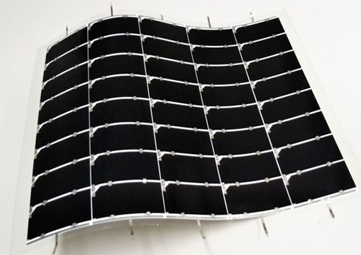
“This is exciting because hybrid perovskites could be the next generation of solar cells,” she said. “The solar cells convert solar energy into electrical energy so it’s a sustainable and environmentally friendly energy source, giving high performance at a low cost.”
Zeev “Valy” Vardeny, co-author and distinguished professor of physics and astronomy, University of Utah, agrees. “This work shows that in addition to solar cell technologies, the hybrid perovskites have potential to be used in a variety of optoelectronic applications.”
This next step in the development of these materials as the possible next generation of solar cell components is detailed in a study published onlineby the two research teams in the journal MRS Communications which also published a news release.
Jurchescu said hybrid perovskites have taken the solar cell field by storm since 2009, when they were first introduced. The power conversion efficiencies have grown from around 4 percent to 20 percent in just five years. By comparison, other conventional materials used to generate electricity from sunlight have taken decades to achieve high performance levels.
Jurchescu and graduate student Yaochuan “Josh” Mei, who has worked in her lab for almost five years, said this research builds on what they have learned in their previous work. “This work is based on the knowledge and infrastructure learned from our organic electronics work over the years,” Mei said. “This material is pretty new for us and we learned a lot in just a few months.”
“We will learn from these first lessons and try to make them better,” Jurchescu said. “Really, this is just the first step. Next we will look into the spin manipulation of the injected carriers in these devices and other electrical, optical and magnetic field applications.”
Co-authors from the University of Utah are Z. Valentine Vardeny and C. Zhang.
The paper:

