27.01.2015
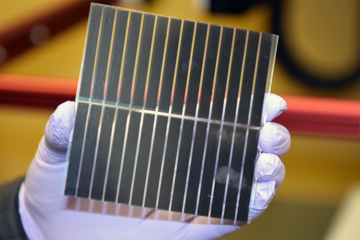
ETH researchers have developed a comprehensive model to explain how electrons flow inside new types of solar cells made of tiny crystals. The model allows for a better understanding of such cells and may help to increase their efficiency.
Scientists are focusing on nanometre-sized crystals for the next generation of solar cells. These nanocrystals have excellent optical properties. Compared with silicon in today’s solar cells, nanocrystals can be designed to absorb a larger fraction of the solar light spectrum. However, the development of nanocrystal-based solar cells is challenging: “These solar cells contain layers of many individual nano-sized crystals, bound together by a molecular glue. Within this nanocrystal composite, the electrons do not flow as well as needed for commercial applications,” explains Vanessa Wood, Professor of Materials and Device Engineering at ETH Zurich. Until now, the physics of electron transport in this complex material system was not understood so it was impossible to systematically engineer better nanocrystal-composites.
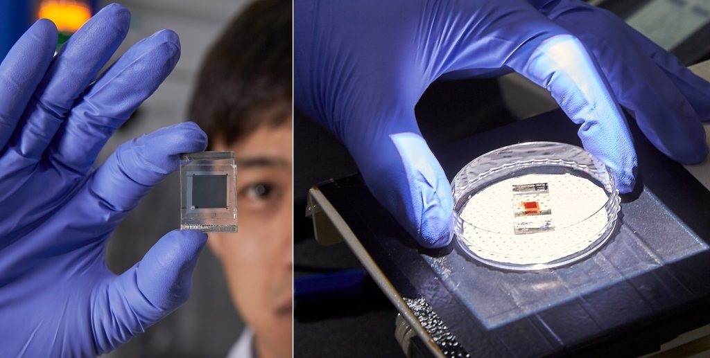
Wood and her colleagues conducted an extensive study of nanocrystal solar cells, which they fabricated and characterized in their laboratories at ETH Zurich. They were able to describe the electron transport in these types of cells via a generally applicable physical model for the first time. “Our model is able to explain the impact of changing nanocrystal size, nanocrystal material, or binder molecules on electron transport,” says Wood. The model will give scientists in the research field a better understanding of the physical processes inside nanocrystal solar cells and enable them to improve solar cell efficiency.
Promising outlook thanks to quantum effects
The reason for the enthusiasm of many solar cell researchers for the tiny crystals is that at small dimensions effects of quantum physics come into play that are not observed in bulk semiconductors. One example is that the physical properties of the nanocrystals depend on their size. And because scientists can easily control nanocrystal size in the fabrication process, they are also able to influence the properties of nanocrystal semiconductors and optimize them for solar cells.
One such property that can be influenced by changing nanocrystal size is the amount of sun’s spectrum that can be absorbed by the nanocrystals and converted to electricity by the solar cell. Semiconductors do not absorb the entire sunlight spectrum, but rather only radiation below a certain wavelength, or – in other words – with an energy greater than the so-called band gap energy of the semiconductor. In most semiconductors, this threshold can only be changed by changing the material. However, for nanocrystal composites, the threshold can be changed simply by changing the size of the individual crystals. Thus scientists can select the size of nanocrystals in such a way that they absorb the maximum amount of light from a broad range of the sunlight spectrum.
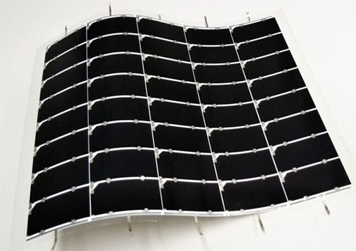
An additional advantage of nanocrystal semiconductors is that they absorb much more sunlight than traditional semiconductors. For example, the absorption coefficient of lead sulfide nanocrystals, used by the ETH researchers in their experimental work, is several orders of magnitude greater than that of silicon semiconductors, used traditionally as solar cells. Thus, a relatively small amount of material is sufficient for the production of nanocrystal solar cells, making it possible to make very thin, flexible solar cells.
Need for greater efficiency
The new model put forth by the ETH researchers answers a series of previously unresolved questions related to electron transport in nanocrystal composites. For example, until now, no experimental evidence existed to prove that the band gap energy of a nanocrystal composite depends directly on the band gap energy of the individual nanocrystals. “For the first time, we have shown experimentally that this is the case,” says Wood.
Over the past five years, scientists have succeeded in greatly increasing the efficiency of nanocrystal solar cells, yet even in the best of these solar cells just 9 percent of the incident sunlight on the cell is converted into electrical energy. “For us to begin to consider commercial applications, we need to achieve an efficiency of at least 15 percent,” explains Wood. Her group’s work brings researchers one step closer to improving the electron transport and solar cells efficiency.
Scientists are focusing on nanometre-sized crystals for the next generation of solar cells. These nanocrystals have excellent optical properties. Compared with silicon in today’s solar cells, nanocrystals can be designed to absorb a larger fraction of the solar light spectrum. However, the development of nanocrystal-based solar cells is challenging: “These solar cells contain layers of many individual nano-sized crystals, bound together by a molecular glue. Within this nanocrystal composite, the electrons do not flow as well as needed for commercial applications,” explains Vanessa Wood, Professor of Materials and Device Engineering at ETH Zurich. Until now, the physics of electron transport in this complex material system was not understood so it was impossible to systematically engineer better nanocrystal-composites.
Literature reference
Bozyigit D, Lin WMM, Yazdani N, Yarema O, Wood V: A quantitative model for charge carrier transport, trapping and recombination in nanocrystal-based solar cells. Nature Communications, 27 January 2015, doi: 10.1038/ncomms7180

