24 February 2014
Researchers at TU Delft have opened the way for the realization of the next generation of high-efficiency, cost-effective and ultra-thin crystalline silicon solar cells. They are the first in the world to come very close (99.8%) to the theoretical limit of absorption enhancement (light trapping) in a broad light spectrum range. Their article on light management in ultra-thin silicon is accepted for publication in the journal ACS Photonics.
PhD-student Andrea Ingenito of the Photovoltaic Materials and Devices (PVMD) group at TU Delft has experimentally demonstrated the theoretical limit of the enhancement of light absorption in a thin semiconductor material. Ingenito used wafers of crystalline silicon and experimentally proved the theoretical prediction of the maximal enhancement of light absorption in a semiconductor material. He is the first in the world to come very close (99.8%) to the theoretical limit of absorption enhancement in a broad light spectrum range. An experimental demonstration of this absorption enhancement limit in solar cells has been elusive for the last thirty years.
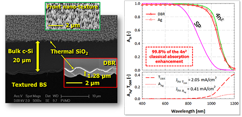
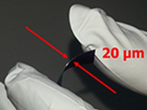
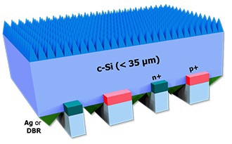
The PVMD group at TU Delft (Faculty of EEMCS) has world-leading expertise in the design, fabrication, and implementation of light trapping structures in the solar cells. The researchers in the group managed to develop an advanced metal-free light trapping scheme for crystalline silicon wafers. At the front side of the silicon wafers they applied a nano-texture known as black-silicon. At the rear side, they implemented a random pyramidal texture coated with a photonic Dielectric Back Reflector which was designed to exhibit maximal and omni-directional internal reflectance. For wafers thinner than 35 μm the researchers achieved more than 99% (with the photonic reflector) and up to 99.8% (with the silver back reflector) of the theoretical classical absorption limit in the broad light spectrum from 400 to 1200 nm.
Successful implementation of TU Delft’s light trapping scheme in crystalline silicon solar cells requires an adequate surface passivation of the front nano-texture. For this purpose, the researchers at the PVMD group have developed thermal silicon oxide and aluminium oxide passivation layers. TU Delft's trapping scheme together with excellent surface passivation opens the way for the realization of the next generation of high-efficiency, cost-effective and ultra-thin crystalline silicon solar cells.
Ingenito’s article in ACS Photonics was co-authored by supervisors prof. dr. Miro Zeman and dr. Olindo Isabella. The research was carried out in the AdLight project (Advanced light trapping for thin and highly efficient silicon solar cells) funded by Agentschap NL. Solland and ECN have been the partners in the project.
Further information
Read here the full publication.
Source:
http://www.tudelft.nl/en/current/latest-news/article/detail/tu-delft-realiseert-maximale-light-trapping-in-zonnecellen/

